Supercharge Your Innovation With Domain-Expert AI Agents!

CRYSTAL, SEMICONDUCTOR ELEMENT, SEMICONDUCTOR DEVICE, and semiconductor system

A semiconductor and oxide semiconductor technology, which is applied in the direction of semiconductor devices, semiconductor/solid-state device components, electrical components, etc., can solve the problem that Schottky electrodes or ohmic electrodes do not work, cannot obtain the electrode structure of semiconductor components, and generate leakage currents And other issues

Pending Publication Date: 2021-07-13
FLOSFIA
View PDF7 Cites 0 Cited by
  • Summary
  • Abstract
  • Description
  • Claims
  • Application Information

AI Technical Summary

Problems solved by technology

[0007] However, when the electrodes described in Patent Documents 1 to 3 are applied to α-Ga 2 o 3 In the case of a semiconductor element used as a semiconductor, there are problems such as that the Schottky electrode or the ohmic electrode does not work, the electrode does not join the film, and the semiconductor characteristics are impaired.
Furthermore, the electrode structures described in Patent Documents 1 to 3 cause leakage current from the electrode ends, etc., and it is not possible to obtain a practically satisfactory electrode structure as a semiconductor element.
[0008] In particular, in recent years, when gallium oxide is used as a semiconductor, Ti / Au is used as an ohmic electrode (Patent Documents 4 to 8), and although good adhesion is shown, the ohmic characteristics are not yet satisfactory. , looking forward to gallium oxide semiconductor elements with excellent ohmic characteristics

Method used


Image

  • CRYSTAL, SEMICONDUCTOR ELEMENT, SEMICONDUCTOR DEVICE, and semiconductor system
  • CRYSTAL, SEMICONDUCTOR ELEMENT, SEMICONDUCTOR DEVICE, and semiconductor system
  • CRYSTAL, SEMICONDUCTOR ELEMENT, SEMICONDUCTOR DEVICE, and semiconductor system

Examples


Embodiment Construction

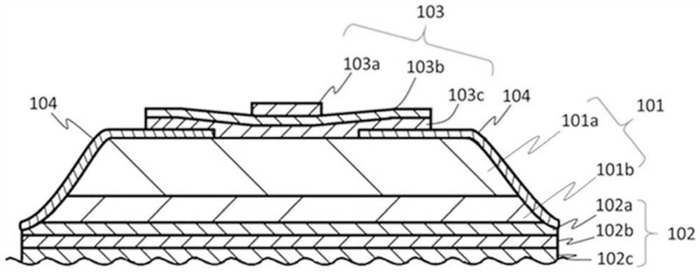
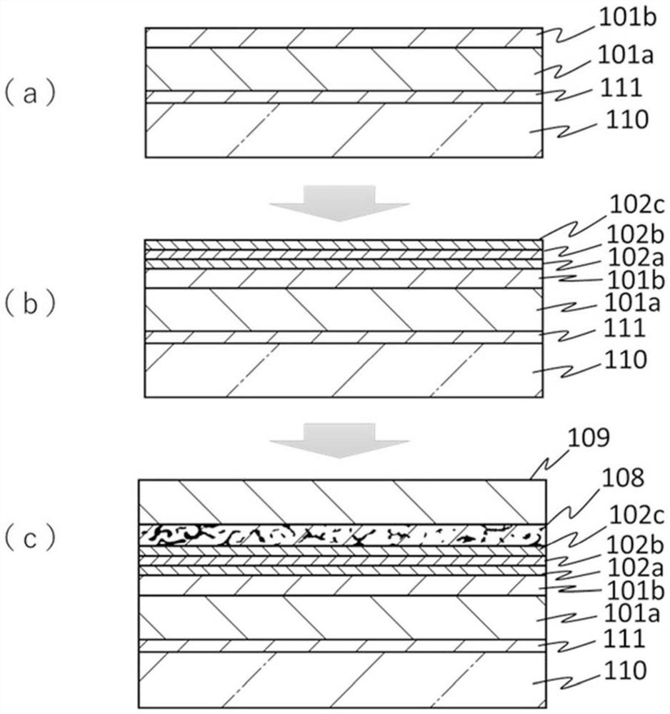
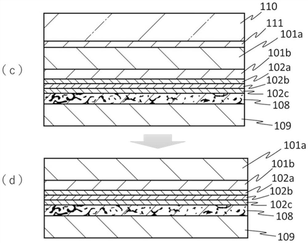
[0059] The crystal of the present invention has a corundum structure, and includes a crystalline oxide as a main component, and the crystalline oxide contains gallium or / and indium, and is characterized in that the crystalline oxide further includes Group 4 of the periodic table of elements Metal. As the Group 4 metal of the periodic table, for example, at least one metal selected from titanium, zirconium, and hafnium can be mentioned, and in the present invention, titanium is preferred. In the present invention, the crystalline oxide preferably contains gallium. The shape of the crystal is not particularly limited, but in the present invention, it is preferably film-like. In addition, the crystals are usually formed by crystal growth, have conductivity, but may also be insulators. It may be a semiconductor including a dopant, a conductor, or a semi-insulator. In the present invention, it is preferable that the crystal has conductivity. In the present invention, when the cr...


PUM


Abstract

The invention relates to a crystal, a semiconductor element, a semiconductor device, and a semiconductor system. The crystal that is useful for the semiconductor element and the semiconductor element that has enhanced electrical properties are provided. The semiconductor element is prepared by the crystal. The crystal, including: a corundum structured crystalline oxide, the crystalline oxide including gallium and / or indium, and the crystalline oxide further including a metal of Group 4 of the periodic table. The crystal is used to make a semiconductor element, and the obtained semiconductor element is used to make a semiconductor device such as a power card. Also, the semiconductor element and the semiconductor device are used to make the semiconductor system.

Description

technical field [0001] The present invention relates to a crystal useful for power devices and the like, a semiconductor element, a semiconductor device and a semiconductor system using the semiconductor element. Background technique [0002] Gallium oxide (Ga 2 o 3 ) has a wide bandgap of 4.8-5.3eV at room temperature and is a transparent semiconductor that hardly absorbs visible light and ultraviolet rays. Therefore, especially as promising materials for use in opto / electrical devices and transparent electronic devices operating in the deep ultraviolet region, in recent years, gallium oxide (Ga 2 o 3 ), photodetectors, light-emitting diodes (LEDs) and transistors (see Non-Patent Document 1). [0003] In addition, in gallium oxide (Ga 2 o 3 ) There are five crystal structures of α, β, γ, σ, ε, and the most stable structure is usually β-Ga 2 o 3 . However, β-Ga 2 o 3 Since it has a β-gallia structure, it is different from the crystal system generally used in elect...

Claims


Application Information

Patent Timeline
IPC IPC(8): H01L29/45H01L29/872
CPCH01L29/45H01L29/872H01L29/24H01L29/66969H02M3/33573H02M3/33576H01L29/0657H02M3/33569H01L23/3675
Inventor 菅野亮平今藤修则松和良加藤勇次
Owner FLOSFIA
Features
  • R&D
  • Intellectual Property
  • Life Sciences
  • Materials
  • Tech Scout
  • Unparalleled Data Quality
  • Higher Quality Content
  • 60% Fewer Hallucinations
Learn More