Silicon carbide device, preparation method thereof and semiconductor device

A technology of silicon carbide and devices, which is applied in semiconductor devices, semiconductor/solid-state device manufacturing, electrical components, etc., and can solve problems such as demanding driving requirements, large leakage currents, and false openings

Active Publication Date: 2021-07-16
BYD SEMICON CO LTD
View PDF10 Cites 1 Cited by
  • Summary
  • Abstract
  • Description
  • Claims
  • Application Information

AI Technical Summary

Problems solved by technology

However, the n epitaxial layer needs to be thinner, otherwise there will be a large leakage in the reverse blocking state, so the manufacturing process requires more precise thickness control; in addition, because the fo

Method used


Image

  • Silicon carbide device, preparation method thereof and semiconductor device
  • Silicon carbide device, preparation method thereof and semiconductor device
  • Silicon carbide device, preparation method thereof and semiconductor device

Examples


Embodiment 1

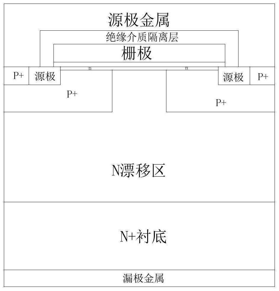
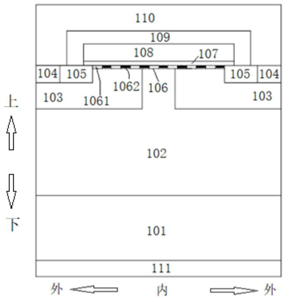
[0043] 1. Epitaxially grow a layer of drift region on the substrate to form a wafer for making silicon carbide devices;

[0044] 2. Form a p-hydrazine region on the upper surface of the wafer by photolithography implantation

[0045] 3. A thin n-type epitaxial layer is epitaxially formed on the surface of the wafer;

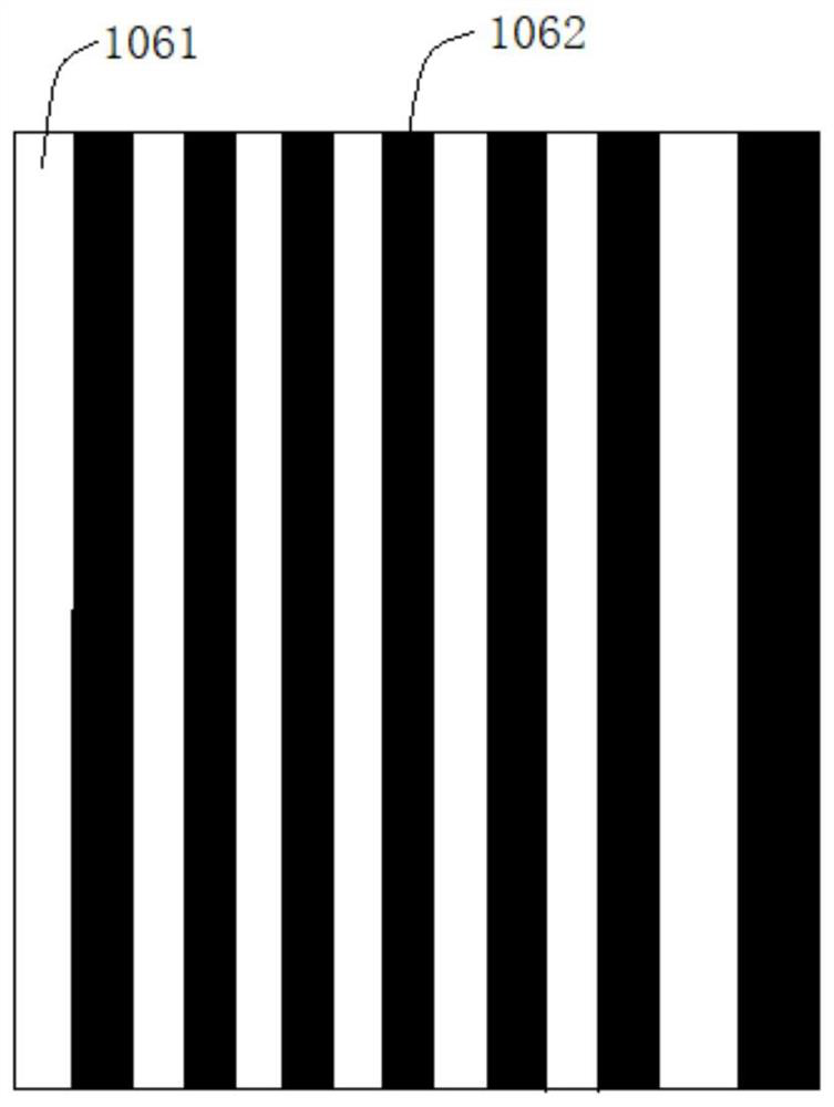
[0046] 4. Impurities are implanted through the photomask to form n-type doped regions 805, and combined with the epitaxial layer formed in the previous step to form p-type doped regions and n-type doped regions alternately arranged and distributed, and the plane of the doped thin layer Structural schematic reference image 3 , and the maximum width of the p-type doped region and the n-type doped region is 0.5 microns;

[0047] 5. The source electrode and P+ contact area of ​​the device are formed by photolithography implantation;

[0048] 6. Grown the gate oxide layer by wet oxidation, deposited polysilicon, formed the gate by photolithography and etching thro...

Embodiment 2

[0051] Same as Example 1, the difference is that the planar structure schematic diagram of the doped thin layer refers to Figure 4 .

Embodiment 3

[0053] Same as Example 1, the difference is that the planar structure schematic diagram of the doped thin layer refers to Image 6 .


PUM

PropertyMeasurementUnit
Maximum widthaaaaaaaaaa

Abstract

The invention provides a silicon carbide device, a preparation method thereof and a semiconductor device. The silicon carbide device comprises a substrate, a drift region which is arranged above the substrate, a well region which is arranged above the drift region, a contact region which is arranged above the well region, a source electrode which is arranged above the well region and is positioned on the inner side of the contact region, and a doped thin layer which is arranged above the well region and the drift region, is positioned on the inner side of the source electrode, and comprises at least one n-type doped region and at least one p-type doped region. The silicon carbide device has relatively small on resistance and leakage current, and meanwhile, the silicon carbide device has relatively high application reliability.

Description

technical field [0001] The present invention relates to the technical field of semiconductor devices, in particular to silicon carbide devices and semiconductor devices containing the same. Background technique [0002] In order to solve the problem of the large channel resistance of silicon carbide MOSFETs, the researchers proposed to grow a thin n-type epitaxial layer by epitaxy after the p-well (p well) region is generated on the device (see the schematic diagram of the structure). figure 1 ), the n-type epitaxial layer forms a high-mobility conductive channel when the device is forward-conducting, reducing the on-resistance. However, the n epitaxial layer needs to be thinner, otherwise there will be a large leakage in the reverse blocking state, so the manufacturing process requires more precise thickness control; in addition, because the forward conduction turn-on voltage is small, it is easy to The risk of false opening occurs, and the requirements for the driver are ...

Claims


Application Information

Patent Timeline
IPC IPC(8): H01L29/78H01L29/06H01L21/04
CPCH01L29/7802H01L29/0619H01L21/0455H01L29/66068
Inventor 朱辉肖秀光
Owner BYD SEMICON CO LTD
Why Eureka
Try Eureka