Selective etching epitaxial Micro-LED chip and design and preparation method thereof

A chip and selection technology, applied in semiconductor/solid-state device manufacturing, semiconductor devices, electrical components, etc., can solve the problems of RGB three-primary color crosstalk, reduce the performance of Micro-LED display, avoid damage, improve color conversion efficiency, improve The effect of radiative recombination efficiency

Active Publication Date: 2021-08-03
JIANGXI ZHAO CHI SEMICON CO LTD
View PDF6 Cites 1 Cited by
  • Summary
  • Abstract
  • Description
  • Claims
  • Application Information

AI Technical Summary

Problems solved by technology

[0004] The use of Micro-LEDs to achieve full-color display requires solving the problem of RGB three primary colors. Compared with the general technology of integrating RGB three primary color LED chips on the same substrate, the use of short-wavelength ultraviolet light to excite nanowires The full-color display solution that achieves color conversion by array light emission does not need to separate monochrome Micro-LED chips on different wafers to form RGB pixels, but it is prone to crosstalk of the three primary colors of RGB, which reduces the display performance of Micro-LEDs

Method used


Image

  • Selective etching epitaxial Micro-LED chip and design and preparation method thereof
  • Selective etching epitaxial Micro-LED chip and design and preparation method thereof
  • Selective etching epitaxial Micro-LED chip and design and preparation method thereof

Examples


Embodiment 1

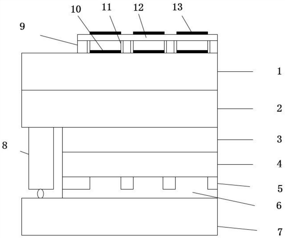
[0035] Provided is a selective etching epitaxy reduction crosstalk full-color Micro-LED array design and preparation method, which specifically includes the following steps:

[0036] S1. Provide a sapphire substrate 1 with a thickness of 200 μm, and use MOCVD technology to sequentially grow an n-GaN layer 2 with a thickness of 3 μm and 5 pairs of Al with a total thickness of 65 nm on the sapphire substrate 0.47 Ga 0.53 N(10nm) / Al 0.57 Ga 0.43N (3nm) multi-quantum well layer 3, p-GaN layer 4 with a thickness of 3 μm;

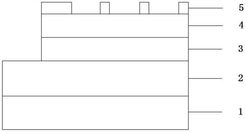
[0037] S2. On the epitaxial structure obtained in S1, the epitaxial structure includes n-GaN layer, multiple quantum well layer, p-GaN layer and deposited SiO 2 Insulating layer, using PECVD technology to deposit SiO with a thickness of 5 μm on p-GaN 2 insulating layer 5, such as figure 2 shown;

[0038] S3. Use photolithography to transfer the pattern on the mask to SiO 2 insulating layer, and then use ICP technique on SiO 2 Selective etching is perform...


PUM

PropertyMeasurementUnit
thicknessaaaaaaaaaa
thicknessaaaaaaaaaa
thicknessaaaaaaaaaa

Abstract

The invention discloses a selective etching epitaxial Micro-LED chip and a design and preparation method thereof. The method specifically comprises the following steps: sequentially growing an n-GaN layer, a multi-quantum well layer and a p-GaN layer on a sapphire substrate, depositing a SiO2 insulating layer, etching a micropore array on the SiO2 insulating layer, realizing isolation of micropore pixel points by utilizing low conductivity of modified p-GaN and current expansion only below the micropore array, and placing a color conversion unit on the substrate. The chip comprises an ultra-black matrix shading layer with the surface coated with Ag, a GaInP nanowire polymer film, an ultraviolet light AlGaN / GaN DBR reflecting mirror and an RGB three-color optical filter, so the Micro-LED chip capable of reducing crosstalk and improving color conversion efficiency is obtained.

Description

technical field [0001] The invention relates to the technical field of semiconductor light emitting devices, in particular to a selective etching epitaxial Micro-LED chip and a design and preparation method thereof. Background technique [0002] When the size of the LED chip is reduced to tens of microns or even a few microns, it is called Micro-LED chip. Micro-LED display is an array display technology composed of micron-scale semiconductor light-emitting units, which is different from traditional OLED and LCD display technologies. In comparison, Micro-LED has the advantages of high brightness, wide color gamut, low energy consumption, fast response time, and high reliability, so it has great potential in wearable devices, augmented reality (AR), virtual reality (VR), visible light communication and other fields. It has a very broad application prospect and is also regarded as the next generation of display technology. [0003] Compared with general large-size LED chips, t...

Claims


Application Information

Patent Timeline
Patent Type & Authority Applications(China)
IPC IPC(8): H01L33/06H01L33/32H01L33/50H01L33/00H01L25/16H01L21/50
CPCH01L33/06H01L33/32H01L33/50H01L33/005H01L25/167H01L25/50
Inventor 周圣军陶国裔万泽洪钱胤佐
Owner JIANGXI ZHAO CHI SEMICON CO LTD
Why Eureka
Try Eureka