Method for inducing crystallization of chalcogenide phase change material and application thereof

A technology of phase change materials and chalcogenides, applied in the field of microelectronics, can solve problems such as poor stability, incompatibility of semiconductor processes, and speed up the crystallization speed of phase change materials, so as to achieve the effect of increasing the crystallization speed

Active Publication Date: 2021-08-10
HUAZHONG UNIV OF SCI & TECH
View PDF11 Cites 2 Cited by
  • Summary
  • Abstract
  • Description
  • Claims
  • Application Information

AI Technical Summary

Problems solved by technology

[0004] The invention provides a method for inducing the crystallization of chalcogenide phase-change materials and its application to solve the technical problems...

Method used


Image

  • Method for inducing crystallization of chalcogenide phase change material and application thereof
  • Method for inducing crystallization of chalcogenide phase change material and application thereof
  • Method for inducing crystallization of chalcogenide phase change material and application thereof

Examples


Embodiment 1

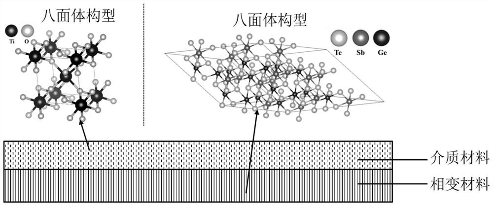
[0024] A method for inducing the crystallization of a chalcogenide phase change material, wherein the dielectric material is in contact with the interface of the chalcogenide phase change material, wherein the structure of the dielectric material is an octahedral configuration, and the dielectric material is a chalcogenide at the interface where the two contact The crystallization of phase change materials provides crystal nucleus growth centers to induce accelerated crystallization of phase change materials.

[0025] At present, most of the crystallization of phase change materials is mainly induced by adjusting the ratio or composition of the material, or doping the material, such as using Sc doping to increase the number of initial four-membered rings in the phase change material, thereby increasing the phase change. However, this method has a series of problems such as poor thermal stability, easy oxidation, immature materials and incompatibility with today's semiconductor ...

Embodiment 2

[0032] A phase-change memory unit, in the memory unit device, among all the dielectric material layers in contact with the chalcogenide phase-change material layer, the dielectric material structure of at least one side of the dielectric material layer is an octahedral configuration; During the crystallization process of the material, the dielectric material provides a crystal nucleus growth center for the crystallization of the chalcogenide phase change material at the contact interface between the two, and accelerates the crystallization process of the phase change material.

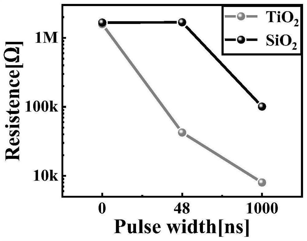
[0033]In the existing memory cell structure, there is a dielectric material in contact with the phase change material, that is, the interface between the dielectric material and the phase change material itself exists. Considering that the crystallization speed of the phase change material and the required applied voltage are phase change functions The core indicators of the layer determine a series of ...

Embodiment 3

[0040] A method for preparing a phase-change memory unit as described in Embodiment 2. During the preparation process, a dielectric material with an octahedral structure is selected as the medium material layer in all dielectric material layers in contact with the chalcogenide phase-change material layer. At least one layer of material.

[0041] Specific examples are given below:

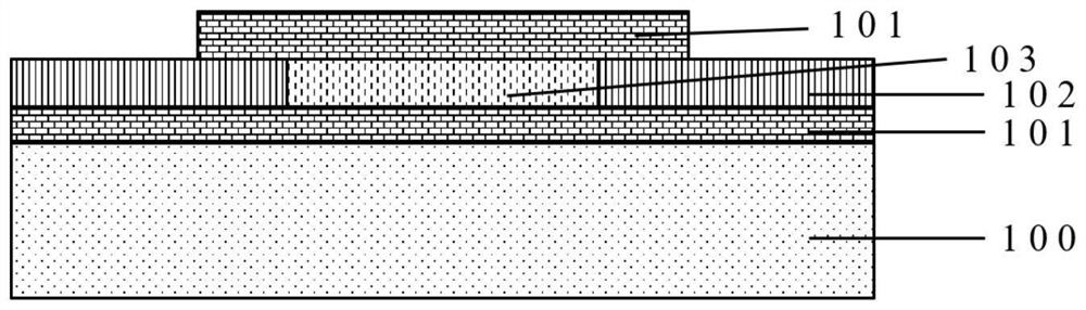
[0042] Such as image 3 The structure of a lateral nanostructure phase-change memory unit shown, the manufacturing steps are:

[0043] Step 1: Carry out photolithography on a silicon substrate (i.e. semiconductor substrate 100) whose crystal orientation is and has a lower dielectric material layer 101 on the surface. The material of the lower dielectric material layer 101 is titanium oxide material, and then A layer of electrode layer 102 is deposited on the engraved substrate by magnetron sputtering coating method, and after stripping, two symmetrical left and right electrodes are obtained. The ...


PUM

PropertyMeasurementUnit
Thicknessaaaaaaaaaa
Thicknessaaaaaaaaaa
Thicknessaaaaaaaaaa

Abstract

The invention belongs to the field of microelectronics, and particularly relates to a method for inducing crystallization of a chalcogenide phase change material and application thereof, wherein specifically, a dielectric material is in interface contact with a chalcogenide phase change material, and the dielectric material is of an octahedral structure, and provides a crystal nucleus growth center for crystallization of the chalcogenide phase change material at the contact interface of the dielectric material and the chalcogenide phase-change material so as to induce accelerated crystallization of the phase-change material. The method is further applied to an existing phase change memory unit, so that the dielectric material structure of at least one dielectric material layer in all dielectric material layers in contact with the chalcogenide phase change material layer is of an octahedral structure. According to the invention, the dielectric material with an octahedral structure is in contact with the interface of the phase change material layer, the contact interface is inherent to a memory unit device and does not need to be additionally introduced, the influence on the whole semiconductor process is reduced to the minimum, and the phase change material is not optimized and modified in the design of the phase change memory unit, so that a series of other problems caused by optimization of the phase change material are avoided.

Description

technical field [0001] The invention belongs to the field of microelectronics, and more specifically relates to a method for inducing the crystallization of a chalcogenide phase-change material and its application. Background technique [0002] With the advent of the information age, people put forward higher and higher requirements for storage speed, and constantly put forward new goals for the research and development of non-volatile memory. As a result, many new storage devices have gradually become research hotspots in academia and industry. Among them, phase change memory has been adopted by International Semiconductor Technology Co., Ltd. due to its relatively simple device structure, high erase and write speed, low power consumption, and excellent storage performance such as radiation resistance. The industry association believes that in the future, it is most likely to replace the current flash memory and become the mainstream product of memory and the first device t...

Claims


Application Information

Patent Timeline
IPC IPC(8): H01L45/00B01D9/00
CPCB01D9/005B01D9/0077H10N70/231
Inventor 童浩赵锐哲缪向水
Owner HUAZHONG UNIV OF SCI & TECH
Why Eureka
Try Eureka