Snapback transient voltage suppressor

A transient voltage suppression, conductive type technology, applied in the direction of electric solid devices, circuits, electrical components, etc., can solve the problems of low clamping voltage, high frequency signal packet loss, etc., to achieve low breakdown voltage and trigger voltage, application Flexible, protective and responsive effects

Inactive Publication Date: 2021-08-13
SHANGHAI CHANGYUAN WAYON MICROELECTRONICS
View PDF4 Cites 1 Cited by
  • Summary
  • Abstract
  • Description
  • Claims
  • Application Information

AI Technical Summary

Problems solved by technology

[0004] At present, integrated circuits continue to develop in the direction of low voltage, low power consumption, and high-speed transmission, and higher performance requirements are put forward for corresponding TVS protection devices. It is required that the clamping voltage of TVS protection devices should be as low as possible, and that The capacitance should be as small as possible. It is usually used in high-speed ports such as HDMI3.0 / 3.1 and USB3.1. The capacitance requirement is less than 0.5pF. Larger capacitance will cause abnormalities such as packet loss during transmission of high-frequency signals.

Method used


Image

  • Snapback transient voltage suppressor
  • Snapback transient voltage suppressor
  • Snapback transient voltage suppressor

Examples


Embodiment 1

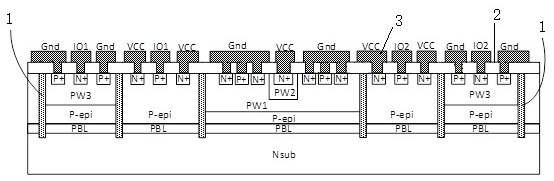
[0046] Embodiment 1: A snapback transient voltage suppressor prepared by the present invention, such as figure 1 As shown, it includes: a substrate; a buried layer formed on the upper surface of the substrate, the conductivity type of the buried layer is different from that of the substrate; an epitaxial layer formed on the upper surface of the buried layer, the conductivity of the epitaxial layer The type is different from the conductivity type of the substrate, that is, the conductivity type of the epitaxial layer is the same as that of the buried layer. If the substrate is an N-type substrate N sub, the epitaxial layer is a P-type epitaxial layer P-epi, and the buried layer is P-epi. type buried layer PBL; if the substrate is a P-type substrate P sub, the epitaxial layer is an N-type epitaxial layer N-epi, and the buried layer is an N-type buried layer NBL. In the epitaxial layer N-epi, the buried layer is an N-type buried layer NBL as an example; a plurality of predetermined...

Embodiment 2

[0070] This embodiment is similar to Embodiment 1, other structures are the same as Embodiment 1, and the manufacturing method is also the same. The difference between this embodiment and Embodiment 1 is that in this embodiment, the first preset area and the fifth preset area The third P-type well region PW3 is removed, and the functions realized by the device remain unchanged. The snapback transient voltage suppressor prepared in this embodiment is as follows: Figure 10As shown, it specifically includes: a substrate; a buried layer formed on the upper surface of the substrate, the conductivity type of the buried layer is different from that of the substrate; an epitaxial layer formed on the upper surface of the buried layer, the epitaxial layer The conductivity type is different from that of the substrate, that is, the conductivity type of the epitaxial layer is the same as that of the buried layer. If the substrate is an N-type substrate N sub, the epitaxial layer is a P-typ...

Embodiment 3

[0072] This embodiment is similar to Embodiment 1, other structures are the same as Embodiment 1, and the manufacturing method is also the same. The difference between this embodiment and Embodiment 1 is that in this embodiment, the first preset area and the fifth preset area The third P-type well region PW3 and the buried layer grown on the substrate are removed, and the functions realized by the device remain unchanged. The snapback transient voltage suppressor prepared in this embodiment is as follows: Figure 11 As shown, it specifically includes: a substrate; an epitaxial layer formed on the upper surface of the substrate, and the conductivity type of the epitaxial layer is different from that of the substrate. If the substrate is an N-type substrate N sub, the epitaxial layer is P-type epitaxial layer P-epi; if the substrate is P-type substrate P sub, the epitaxial layer is N-type epitaxial layer N-epi; multiple predetermined regions are formed in the epitaxial layer, and...


PUM

PropertyMeasurementUnit
Thicknessaaaaaaaaaa
Depthaaaaaaaaaa
Widthaaaaaaaaaa

Abstract

The invention discloses a snapback transient voltage suppressor, and belongs to the field of semiconductor protection devices. The suppressor comprises: an epitaxial layer formed on a substrate; a plurality of preset regions formed in the epitaxial layer and isolated by an isolation structures, wherein the first preset region and the fifth preset region comprise a first P+ region, a first N+ region and a second P+ region, the second preset region and the fourth preset region comprise a second N+ region, a third P+ region and a third N+ region, and the third preset region comprises a first P-type well region, a second P-type well region, a fourth N+ region formed in the second P-type well region, and two fourth P+ regions and two fifth N+ regions formed in the first P-type well region; a dielectric layer formed on the upper surface of the epitaxial layer, wherein the dielectric layer comprises metal holes corresponding to the P+ regions and the N+ regions; and a plurality of metal layers formed in each of the metal holes. The suppressor has the beneficial effects that the breakdown voltage and the trigger voltage are lower, the protection response is faster, the on resistance and the clamping voltage are smaller, and the protection capability for a post-stage integrated circuit is stronger.

Description

technical field [0001] The invention relates to the field of semiconductor protection devices, in particular to the field of design and manufacture of protection devices for high-speed signal ports, and in particular to a low-capacitance small snapback transient voltage suppressor. Background technique [0002] Transient Voltage Suppressor (TVS) is a high-efficiency clamp overvoltage protection device in the form of a diode. When the two poles of the TVS diode are impacted by reverse transient high energy, it can change the high impedance between its two poles to low impedance at a speed of 10 minus 12 seconds, absorbing surge power up to several thousand watts , so that the voltage between the two poles is clamped at a predetermined value, and the predetermined value is at a relatively low voltage level, so that the post-stage integrated circuit is protected from the impact of electrostatic discharge or surge voltage, and effectively protects the precision components in the...

Claims


Application Information

Patent Timeline
IPC IPC(8): H01L27/02
CPCH01L27/0255H01L27/0259
Inventor 蒋骞苑赵德益吕海凤张啸王允郝壮壮胡亚莉李佳豪张彩霞
Owner SHANGHAI CHANGYUAN WAYON MICROELECTRONICS
Why Eureka
Try Eureka