
Collimating film and preparation method of collimating film

A technology of collimating lens and straight hole, applied in the field of image recognition, can solve the problem of difficult alignment of two-layer collimating diaphragms, and achieve the effects of improved mass production, low thickness and accurate alignment

Pending Publication Date: 2021-08-24
NINGBO EXCITON TECH
View PDF0 Cites 13 Cited by
  • Summary
  • Abstract
  • Description
  • Claims
  • Application Information

AI Technical Summary

Problems solved by technology

[0007] In order to solve the problem of difficult alignment of two layers of collimating diaphragms in traditional rigid collimating sheets, the present invention provides a collimating film and its preparation method
The collimating film provided by the present invention only includes one layer of collimating holes, which solves the problem of difficult alignment of two layers of collimating diaphragms

Method used


Image

  • Collimating film and preparation method of collimating film
  • Collimating film and preparation method of collimating film
  • Collimating film and preparation method of collimating film

Examples


Embodiment 1

[0135] like Image 6 The display is shown in the present invention, including the collimating lens layer 41, the flexible substrate layer 42, and the collisional, the collimated lens layer is placed on the upper surface of the substrate, the collimated hole layer is placed in the lower surface of the substrate. The aligned direct lens layer 41 includes a microbial array 41a and a thickness 41b, and the pore layer 43 includes a collimated pore array formed after the light-shielding medium 43a and the dielectric hollow (constitute a certain number of quantity pores 43b); The thickness T of the flexible matrix layer is 25 μm. The collimated lens arrays and collimated pore arrays are closely arranged in a normal triangle array (eg Figure 8 Indicated). The main optical axis of the microlens is 18 μm, the radius of curvature R is 12.6 μm, the collimation lens layer thickness H is 8.5 μm, and the thickness T of the straight hole layer is 2 μm, the collimated hole diameter φ is 4 μm. . The...

Embodiment 2-24

[0144] As shown in Example 1, the collimated lens array and the collimated pore array in the collimator are closely arranged in a positive triangle, and the material of the straight lens layer 41 is PMMA, the flexible matrix layer 42. The light shielding medium 43a of the colored hole layer 43 is the inorganic coating, which is collected by the microlens in a microbial punch. The other parameters are listed in Table 1.

[0145] Table 1 Examples 1 to 24 design parameters and optical properties

[0146]

[0147]

[0148] Note 1: P is the minimum spacing of the main optical axis of the microlens, the unit μm; R is the radius of curvature of the microlens, the unit μm; H is the thickness of the collimation lens layer, the unit μm; N1 is the refractive index of the collimation lens layer, no quantity The unit; T is the thickness of the flexible matrix layer, the unit μm; N2 is the refractive index of the flexible matrix layer, and the dimensiony unit; D is a spot diameter formed on...

Embodiment 25-30

[0151] As shown in Example 1, the column of the straight film is closely arranged in a positive triangle, and the material of the straight lens layer 41 is a material of PMMA and a material of the flexible matrix. For the PET, the light shielding medium 43a of the collimating hole layer 43 is a inorganic coating carbide, the ratio of the metallic film, which is collected by the microlens, and the other parameters are listed in Table 2.

[0152] Table 2 Embodiments 25 to 30 design parameters and optical properties

[0153]

[0154] Note 1 with Table 1.

[0155] As shown in Table 2, embodiments 25 to 30 are different from different flexible substrates. Examples 25 to 27 are p = 10 μm, and the other parameter is unchanged, T = 10, 15, 20 μm is a set of quasi-metallic films, and Examples 28 to 30 are P = 25 μm, respectively, and other parameters constant Next, T = 25, 38, 50 μm is another set of quasi-straight film. When t is increasing, in order to keep the microsocratic effect (th...


PUM

PropertyMeasurementUnit
radiusaaaaaaaaaa
heightaaaaaaaaaa
thicknessaaaaaaaaaa

Abstract

The invention relates to a collimating film, in particular to a collimating film in the field of image recognition and a preparation method of the collimating film. In order to solve the problem that two layers of collimating diaphragms in a traditional rigid collimating sheet are difficult to align, the invention provides a collimating film and a preparation method of the collimating film. The collimating film sequentially comprises a collimating lens layer, a flexible substrate layer and a collimating hole layer; the collimating lens layer comprises a micro-lens array and a lens layer, and the collimating hole layer comprises a collimating hole array; the distribution of the collimation hole array is completely consistent with that of the micro-lens array; and the micro lens arrays of the collimating lens layer are arranged in order. The collimating film provided by the invention only comprises one collimating hole layer, so that the problem that two collimating diaphragms are difficult to align is solved. The collimating film can collimate and filter diffused light at a single-point pixel of an image to a certain extent to form a normal small-beam optical signal, transmits the normal small-beam optical signal to a corresponding photoelectric sensor, and is particularly suitable for a large-size, ultrathin and even flexible image recognition module.

Description

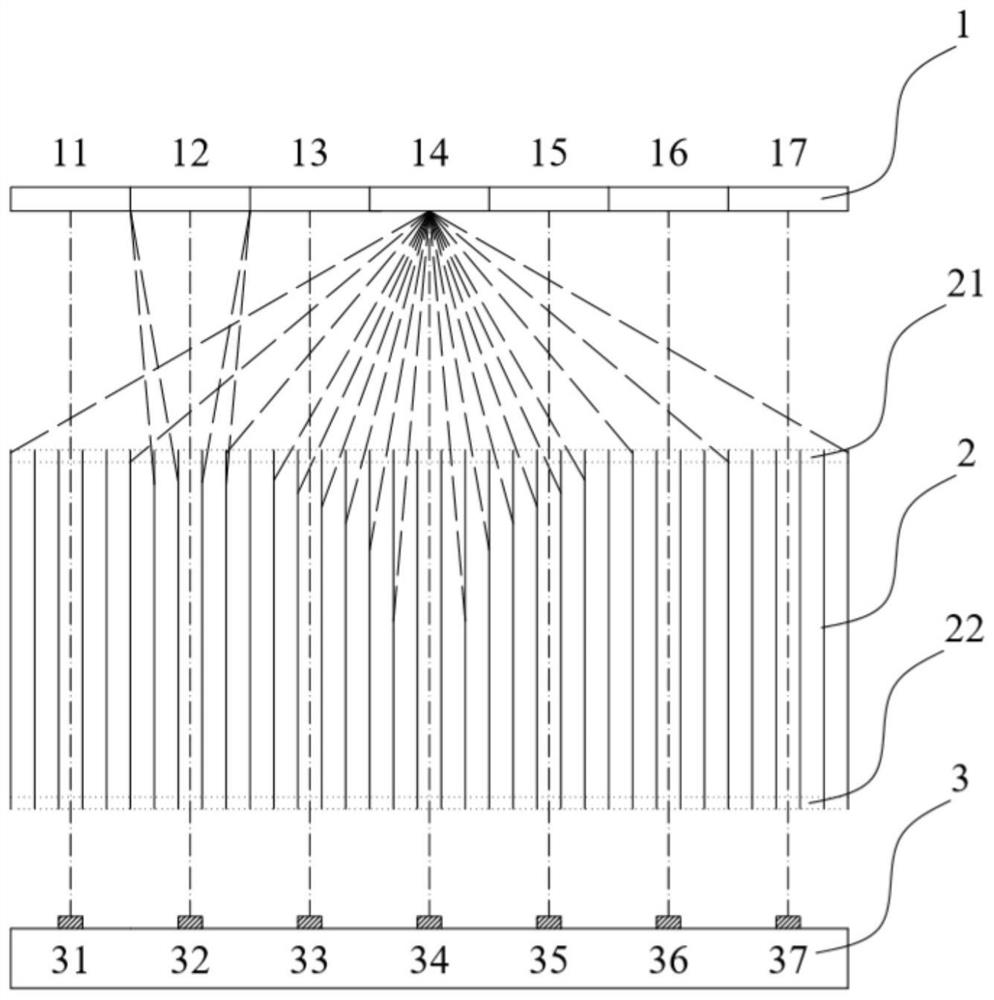
Technical field [0001] The present invention relates to a collimated film, and more particularly to a collimal film and a preparation method thereof in the field of image recognition. Background technique [0002] In the field of image recognition, commonly used image sensors such as CMOS or Photo-TFT types, generally contain collimated devices in the sensor module to enhance signal-to-noise ratio, improve the identification, and reduce crosstalk. The function of collimating devices (such as figure 1 As shown, it is primarily that the diffused light at the image single point pixel is collimated, the collimation light or close to the collimated light (signal), which can be smoothly transmitted, and the deviation method The large angular light (noise) can only be very least even unable to enter the non-corresponding photoactive device, thereby reinforcing it. [0003] Color devices typically have top collimating structures and bottom collimating structures: First, the top and under...

Claims


Application Information

Patent Timeline
Patent Type & Authority Applications(China)
IPC IPC(8): G02B27/30G02B3/00
CPCG02B27/30G02B3/0037G02B3/00
Inventor 李刚夏寅付坤高斌基王小凯陈建文唐海江张彦
Owner NINGBO EXCITON TECH
Learn More