Superconducting transition edge detector and preparation method thereof

A detector, superconducting technology, applied in the field of superconducting electronics

Active Publication Date: 2021-08-24
SHANGHAI TECH UNIV
View PDF9 Cites 2 Cited by
  • Summary
  • Abstract
  • Description
  • Claims
  • Application Information

AI Technical Summary

Problems solved by technology

However, it is a great challenge to prepare TES detectors with high energy resolution, large array, high consistency and high repeatability.

Method used


Image

  • Superconducting transition edge detector and preparation method thereof
  • Superconducting transition edge detector and preparation method thereof
  • Superconducting transition edge detector and preparation method thereof

Examples


preparation example Construction

[0070] The first aspect of the present invention provides a method for preparing a superconducting transition edge detector, comprising:

[0071] 1) forming cut-off layers on both sides of the substrate;

[0072] 2) forming thin film layers on the cut-off layers on both sides;

[0073] 3) forming a superconducting material layer on one side of the film layer;

[0074] 4) forming normal metal strips and / or normal metal points on the edge and / or upper surface of the superconducting material layer;

[0075] 5) forming a heat sink on the film layer on one side of the superconducting material layer;

[0076] 6) forming an absorber on the upper surface of the superconducting material layer;

[0077] 7) Etching to form the edge of the superconducting transition edge detector;

[0078] 8) Etching the backside of the chip.

[0079] In the present invention, in order to alleviate the problem of kink lines appearing at the superconducting transition edge, normal metal strips are gro...

Embodiment 1

[0095] A method for designing and preparing a TES detector suitable for X-ray energy spectrometer applications, comprising the following steps:

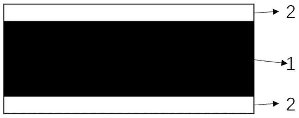
[0096] Step 1): prepare a double-sided polished silicon substrate 1, the thickness of silicon is 400um, such as figure 1 shown;

[0097] Step 2): Use low-pressure chemical vapor deposition to grow a silicon dioxide film 2 on both sides of the silicon substrate with a thickness of 500nm. The side view is as follows figure 2 shown;

[0098] Step 3): grow a low-stress silicon nitride film 3 on the silicon dioxide film 2 on both sides of the silicon substrate, with a thickness of 1um, and the side view is as follows image 3 shown;

[0099] Step 4): Molybdenum structures 4 and copper structures 5 are successively grown on the side where the silicon dioxide and silicon nitride films 3 have been grown using magnetron sputtering, with thicknesses of 60nm and 200nm respectively. The side view is as follows Figure 4 shown;

[0100] Ste...


PUM

PropertyMeasurementUnit
thicknessaaaaaaaaaa
thicknessaaaaaaaaaa
thicknessaaaaaaaaaa

Abstract

The invention relates to the technical field of superconducting electronics, in particular to a superconducting transition edge detector and a preparation method thereof. According to the preparation method provided by the invention, a cut-off layer, a thin film layer, a superconducting material layer, a normal metal strip and/or a normal metal point, a heat sink piece, an absorber and other components are prepared on a substrate in sequence. In the invention, in order to alleviate the problem that a twisted broken line appears at a superconducting transition edge, a normal metal strip grows above a superconducting thin film of a TES detector and some normal metal points are properly added, and in order to reduce the complexity during preparation of the detector and solve the problem of superconductor quenching, an absorber is in direct contact with a superconducting material layer (superconducting thin film), the thickness of a molybdenum thin film is increased when the superconducting thin film is prepared, and the superconducting transition temperature of the detector is regulated and controlled through two sub-layers of the superconducting material layer and three layers of thin films of the absorber.

Description

technical field [0001] The invention relates to the technical field of superconducting electronics, in particular to a superconducting transition edge detector and a preparation method thereof. Background technique [0002] Superconducting Transition Edge Sensor (TES: Transition Edge Sensor) is a new type of superconducting detector developed in recent years. Its energy resolution can reach 1-2eV or even sub-eV, which is two times higher than that of silicon drift detectors. On the other hand, it can be integrated into a large-area multi-element array, so the acceptance angle and effective detection area of ​​the detector are greatly increased, and the detection efficiency can be improved by two orders of magnitude compared with the grating. Because it has the characteristics of high energy resolution and high detection efficiency at the same time, it has become the key deployment target of many advanced X-ray light sources. However, it is a huge challenge to prepare TES de...

Claims


Application Information

Patent Timeline
Patent Type & Authority Applications(China)
IPC IPC(8): H01L39/24H01L39/02G01T1/36
CPCG01T1/366H10N60/80H10N60/01Y02P70/50
Inventor 宋艳汝杨瑾屏张硕夏经铠刘志
Owner SHANGHAI TECH UNIV
Why Eureka
Try Eureka