Optical film for enhancing reflection and direct type backlight module applying same

A technology of optical film and backlight module, which is applied in the field of optical materials and optical systems, and can solve the problems of affecting display effect, color shift of picture quality, increasing product cost and power consumption, etc.

Pending Publication Date: 2021-08-31
SHENZHEN LONGLI TECH CO LTD
View PDF8 Cites 2 Cited by
  • Summary
  • Abstract
  • Description
  • Claims
  • Application Information

AI Technical Summary

Problems solved by technology

However, it is difficult for light to penetrate through the connection position of the reflective cup structure, thus forming a light spot (mura), which affects the display effect
In addition, most conventional Mini-LEDs adopt the COB (full name in English: chip on board) method of cover packaging. Due to the difference in optical path and the waveguide effect of light in the film material during the light emitting process of the Mini-LED chip, each The light type range of the area and the color difference between the borders cause the display brightness to have light and dark differences and color cast of image quality
People try to overcome this defect by adjusting the channel brightness algorithm. However, in the case of mature technical solutions, such algorithms need to be adjusted according to different pictures, which will increase the cost and power consumption of the product. Therefore, this solution is not suitable. Capable of mass production

Method used


Image

  • Optical film for enhancing reflection and direct type backlight module applying same
  • Optical film for enhancing reflection and direct type backlight module applying same
  • Optical film for enhancing reflection and direct type backlight module applying same

Examples


Embodiment 1

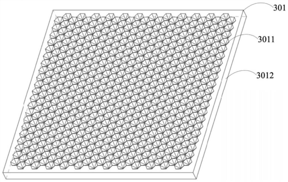
[0046] This embodiment provides an optical film 301 made of polycarbonate, such as image 3 , Figure 4 As shown, the optical film 301 includes a light-emitting side and a light-incident side disposed opposite to each other perpendicular to its thickness direction, a reflective layer 3011 is disposed on the light-emitting side, and a transmissive layer 3012 is disposed on the light-incident side. The surface of the reflective layer 3011 is provided with a plurality of microlens structures that are concave to the inside of the optical film 301. The microlens structures are planar symmetric structures in the shape of hexagonal pyramids, and the size of all the microlens structures is greater than 100 μm. The microlens structure adjoins at least one other microlens structure. In other embodiments, the microlens structure disposed on the reflective layer 3011 may also be other planar symmetric structures, such as a hemispherical structure, a cylindrical structure, a near-conical ...

Embodiment 2

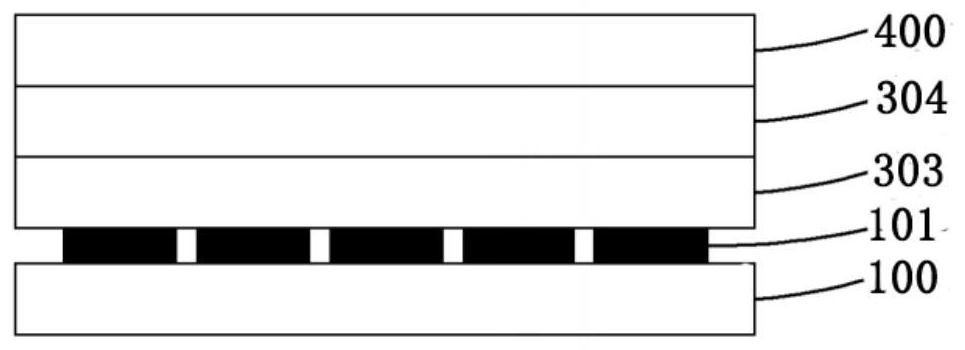
[0054] This embodiment provides a direct-lit backlight device using the optical film 301 provided in Embodiment 1, such as Figure 7 As shown, the direct-lit backlight device further includes a PCB substrate 100 , a reflector 200 and a quantum dot film 303 . A plurality of Mini-LED light sources 101 are installed on the surface of the PCB substrate 100, and the plurality of Mini-LED light sources 101 are arranged periodically. The "periodic arrangement" mentioned here means arranged in a matrix. In this implementation, each Mini-LED - The LED light source 101 comprises a Mini-LED chip. The reflection cover 200 includes a plurality of reflection cup structures with upper and lower openings. In the direct-lit backlight device, the PCB substrate 100, the reflector 200, the optical film 301, and the quantum dot film 303 are arranged sequentially from bottom to top, and each Mini-LED light source 101 is set corresponding to a reflective cup structure. The Mini-LED light source 10...

Embodiment 3

[0060] In the following, only the differences between this embodiment and Embodiment 1 will be described, and the similarities will not be repeated here. This embodiment is based on the optical film structure provided in Example 1, with the ratio of the thickness of the transmissive layer 3012 and the reflective layer 3011 in the optical film as a variable (controlling the thickness of the reflective layer 3011 is constant, by changing the thickness of the transmissive layer 3012 In order to adjust the thickness ratio), different optical films were designed, and the different optical films were assembled with reference to Example 2 in a direct-type backlight device, and the optical performance test was carried out.

[0061] The ratios of the thicknesses of the direct-type backlight device and its optical film of the transmissive layer 3012 to the reflective layer 3011 are respectively: backlight device 1A, transmissive layer: reflective layer = 1:10; backlight device 1B, transm...


PUM

PropertyMeasurementUnit
sizeaaaaaaaaaa
transmittivityaaaaaaaaaa

Abstract

The invention provides an optical film for enhancing reflection. The optical film comprises two side surfaces which are perpendicular to the thickness direction of the optical film and are arranged back to back, and the two side surfaces are respectively marked as a light emergent side and a light incident side; a plurality of micro-lens structures are arranged on the light emitting side to form a reflecting layer with a certain thickness, and the height of the micro-lens structures is the thickness of the reflecting layer; and a film layer between the light incident side and the reflecting layer is used as a transmission layer; a surface, relative to the light-emitting side, of the micro-lens structure is recessed to form a cavity used for being filled with an air medium, and the refractive index of the optical film is larger than that of air, so part of light entering the optical film from the light-incident side can be reflected by the micro-lens structure. By arranging the reflecting layer with the concave micro-lens structure, part of light rays incident from the light incident side of the optical film can be totally reflected, if a reflecting element is arranged on the light incident side of the optical film, the light rays can be reflected for multiple times between the reflecting element and the optical film, and the optical light mixing distance of the light rays is greatly increased.

Description

technical field [0001] The invention belongs to the field of optical materials and optical systems, and in particular relates to an optical film for enhanced reflection and a direct-type backlight module using the same. Background technique [0002] The liquid crystal panel itself included in the liquid crystal display device does not emit light. Therefore, in the liquid crystal display device, a backlight device serving as a surface light source device is provided on the back side of the liquid crystal panel as a light source for illuminating the liquid crystal panel. Mini-light-emitting diodes (Mini-LEDs), which can be used for surface light source backlighting, have attracted much attention due to their advantages of high brightness, high resolution and long life. The Mini-LED chip size is below 200 microns, which can be compared to OLED products in terms of practical effect, and can be more competitive than OLED in terms of material cost, so it has been proposed for use...

Claims


Application Information

Patent Timeline
Patent Type & Authority Applications(China)
IPC IPC(8): G02B3/00G02B1/04G02F1/13357
CPCG02F1/133611G02F1/133605G02F1/133606G02F1/133603G02B1/041G02B3/0056
Inventor 张小齐庄世强彭益
Owner SHENZHEN LONGLI TECH CO LTD
Why Eureka
Try Eureka