Sensor monocrystalline silicon etching device

An etching device and technology of single crystal silicon, applied in the field of sensors, can solve problems such as inability to adjust, fixed distance, uneven etching of sensor single crystal silicon, etc., and achieve the effect of increased loss

Inactive Publication Date: 2021-09-03
徐丽红
View PDF0 Cites 0 Cited by
  • Summary
  • Abstract
  • Description
  • Claims
  • Application Information

AI Technical Summary

Problems solved by technology

[0003] The existing etching device uses a straight cylindrical reaction vessel, and the electric field generated by the electromagnetic coil cooperates with the reaction gas to etch the monocrystalline silicon. During the processing, the chip holder usually needs to be rotated during etching to increase The contact with the plasma is uniform. However, in the current etching process, the distance between the coils on the etching device is fixed and cannot be adjusted. The gas is uniform, which will lead to uneven etching of the sensor monocrystalline silicon on the chip frame. After the etching is completed, some sensor monocrystalline silicon has not been fully etched.

Method used


Image

  • Sensor monocrystalline silicon etching device
  • Sensor monocrystalline silicon etching device
  • Sensor monocrystalline silicon etching device

Examples


Embodiment 1

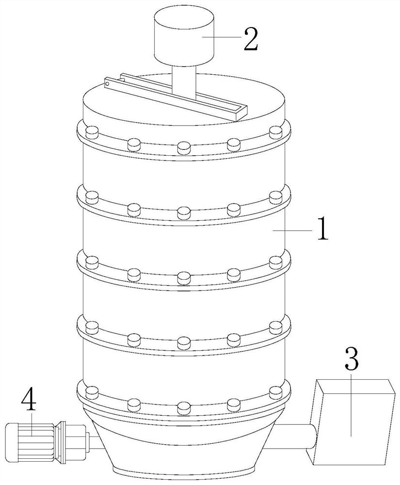
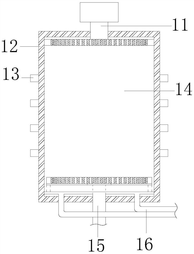
[0024] as attached figure 1 To attach Figure 5 Shown:

[0025] The present invention provides a single crystal silicon etching device for sensors, the structure of which includes an etching mechanism 1, a gas source chamber 2, a vacuum pump 3, and a drive motor 4. The lower end of the gas source chamber 2 is flange-connected to the upper end of the etching mechanism 1, The vacuum pump 3 is arranged on the right side below the air source chamber 2, the driving motor 4 is arranged on the left side below the air source chamber 2, and the etching mechanism 1 is composed of an air supply port 11, a housing 12, an electromagnetic coil 13, and a reaction chamber. The mechanism 14, the first rotating shaft 15, and the suction pipe 16 are composed of the lower end of the air delivery port 11 and the upper end of the housing 12 by welding, the electromagnetic coil 13 is connected with the housing 12 by bolts, and the reaction chamber mechanism 14 is located at the air delivery port ...

Embodiment 2

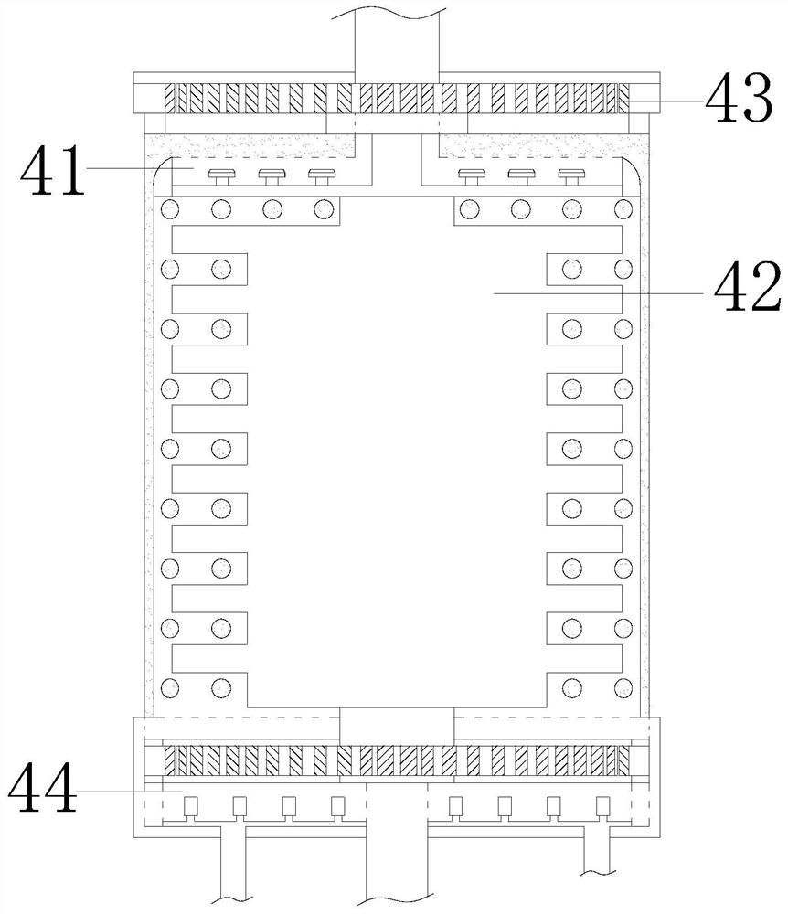
[0032] as attached Figure 6 To attach Figure 7 Shown:

[0033] Wherein, the air suction mechanism 44 is composed of a transmission gear 441, a filter screen 442, an air suction chamber 443, an air suction head mechanism 444, and an air suction pipe 445. The filter screen 442 is arranged on the left and right sides of the transmission gear 441 lower end, so The upper end of the suction chamber 443 is welded to the connecting rod at the lower end of the transmission gear 441, the suction head mechanism 444 is arranged above the inner bottom plate of the suction chamber 443, and the lower end of the suction head mechanism 444 is welded to the upper section of the suction pipe 445, The suction head mechanism 444 is located at the lower end of the housing 12, and the filter screen 442 has properties such as acid resistance, alkali resistance, temperature resistance, and wear resistance, and is used to filter the moisture in the gas so that it enters the suction chamber 443. The g...


PUM


Abstract

The invention discloses a sensor monocrystalline silicon etching device which structurally comprises an etching mechanism, a gas source chamber, a vacuum pump and a driving motor, wherein the lower end of the gas source chamber is connected with a flange at the upper end of the etching mechanism, the vacuum pump is arranged on the right side below the gas source chamber, the driving motor is arranged on the left side below the gas source chamber, the driving motor drives a reaction chamber mechanism in the etching mechanism to rotate in a shell, the gas source chamber conveys gas through a gas supply port, the gas is conveyed into a wafer rack mechanism through a gas distribution net of the gas supply mechanism, the gas generates glow discharge under the action of an electromagnetic coil, the reaction gas and an etched material generate a chemical reaction, and the wafer rack rotates during etching, so that an etched material can be etched more sufficiently, volatile compounds which can be taken away by a gas suction mechanism are generated, chemical etching is realized, and the vacuum pump sucks the volatile compounds in the gas suction mechanism through the gas suction pipeline to reach the maximum vacuum degree.

Description

technical field [0001] The invention relates to the field of sensors, in particular to a sensor single crystal silicon etching device. Background technique [0002] During the processing of monocrystalline silicon for sensors, it needs to be etched; in the existing etching process, it is often done by stacking multiple monocrystalline silicon A reactive gas is introduced into the position, and the reactive gas is made to generate plasma in an electric field environment, so as to etch the single crystal silicon. [0003] The existing etching device uses a straight cylindrical reaction vessel, and the electric field generated by the electromagnetic coil cooperates with the reaction gas to etch the monocrystalline silicon. During the processing, the chip holder usually needs to be rotated during etching to increase The contact with the plasma is uniform. However, in the current etching process, the distance between the coils on the etching device is fixed and cannot be adjuste...

Claims


Application Information

Patent Timeline
Patent Type & Authority Applications(China)
IPC IPC(8): C30B33/12C30B29/06
CPCC30B33/12C30B29/06
Inventor 徐丽红
Owner 徐丽红
Why Eureka
Try Eureka