Transparent conductive film and preparation method and application thereof

A technology of transparent conductive film and transparent substrate, which is applied in the direction of cable/conductor manufacturing, conductive layer on insulating carrier, circuit, etc., and can solve the problems of silver nanowire vulcanization and silver ion migration inhibition effect are not significant, environmental pollution, cost Increase and other issues, to achieve one-dimensional morphology enhancement, improve anti-sulfurization, anti-silver ion migration, and erosion enhancement effects

Pending Publication Date: 2021-09-07
SHENZHEN INST OF ADVANCED ELECTRONICS MATERIALS
View PDF7 Cites 2 Cited by
  • Summary
  • Abstract
  • Description
  • Claims
  • Application Information

AI Technical Summary

Problems solved by technology

However, these methods increase the components of the silver nanowire ink formulation, which leads to an increase in cost and may also cause...

Method used


Image

  • Transparent conductive film and preparation method and application thereof
  • Transparent conductive film and preparation method and application thereof
  • Transparent conductive film and preparation method and application thereof

Examples


Embodiment 1

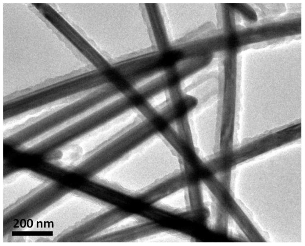
[0033] First, use a wire rod to coat the silver nanowire dispersion in isopropanol on the PET surface, and dry it at 80°C for 5 minutes to evaporate the solvent; then, scrape-coat the tetraethyl orthosilicate on the surface of the silver nanowire network, and then soak it in a 60°C In an aqueous sodium hydroxide solution with a pH of 10, keep warm for 30 minutes; finally, dry to obtain a silver nanowire transparent conductive film. Tested by transmission electron microscopy, such as figure 1 As shown, the surface of silver nanowires can form a silica shell. Hydrogen sulfide treatment for 500 hours, the change in the square resistance of the conductive film is 0.2%; 30V DC voltage treatment for 500 hours, the change in the square resistance of the conductive film is 0.5%; 10% hydrochloric acid solution treatment for 1000 hours, the change in the square resistance of the conductive film is 0.7%; 10% hydrogen Sodium oxide solution treatment for 1000 hours, the change in square r...

Embodiment 2

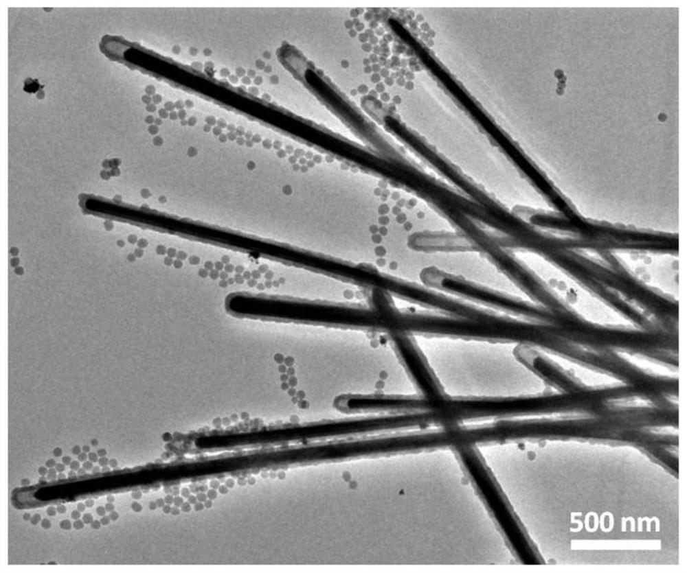
[0035] The silver nanowire transparent conductive film was prepared in the same manner as in Example 1 except that the pH of the aqueous sodium hydroxide solution was 12. Tested by transmission electron microscopy, such as figure 2 As shown, the surface of silver nanowires can form a silica shell. Hydrogen sulfide treatment for 500 hours, the change in the square resistance of the conductive film is 0.3%; 30V DC voltage treatment for 500 hours, the change in the square resistance of the conductive film is 0.6%; 10% hydrochloric acid solution treatment for 1000 hours, the change in the square resistance of the conductive film is 0.6%; 10% hydrogen Sodium oxide solution treatment for 1000 hours, the change in square resistance of the conductive film is 0.5%; treatment at 300°C for 30 minutes, the change in square resistance of the conductive film is 4%.

Embodiment 3

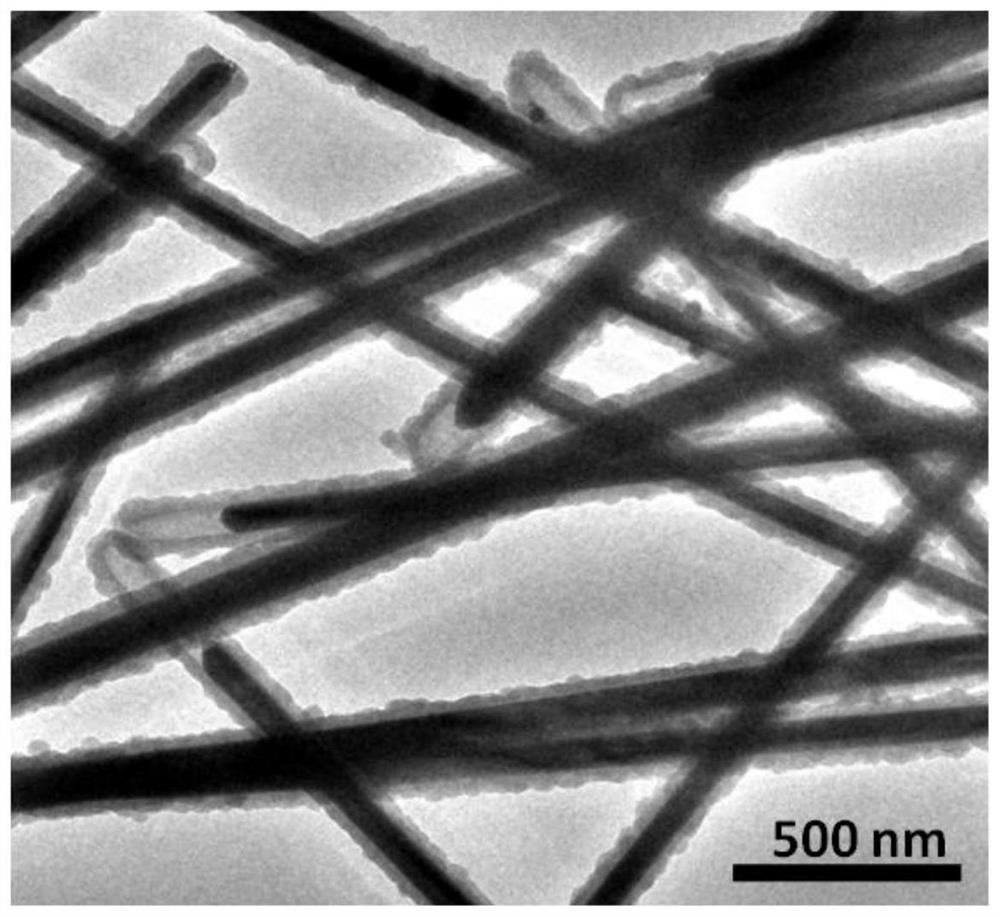
[0037] The silver nanowire transparent conductive film was prepared in the same manner as in Example 1 except that the pH of the sodium hydroxide aqueous solution was 8. Tested by transmission electron microscopy, such as image 3 As shown, the surface of silver nanowires can form a silica shell. Hydrogen sulfide treatment for 500 hours, the change in the square resistance of the conductive film is 0.1%; 30V DC voltage treatment for 500 hours, the change in the square resistance of the conductive film is 0.5%; 10% hydrochloric acid solution treatment for 1000 hours, the change in the square resistance of the conductive film is 0.5%; 10% hydrogen Sodium oxide solution treatment for 1000 hours, the change in square resistance of the conductive film is 0.8%; treatment at 300°C for 30 minutes, the change in square resistance of the conductive film is 3%.


PUM


Abstract

The invention discloses a transparent conductive film as well as a preparation method and application thereof, and particularly relates to a preparation method of a silver nanowire transparent conductive film. The method comprises the following steps: coating a silver nanowire dispersion liquid on the surface of a transparent substrate, and volatilizing a solvent; then coating the surface of the silver nanowire network with a silane coupling agent, soaking the silver nanowire network in an alkaline aqueous solution, preserving heat at 30-100 DEG C for 1-60 minutes, and performing in-situ hydrolytic polycondensation on the silane coupling agent to form a compact silicon dioxide coating layer on the surface of the nanowire; and finally, performing drying to obtain the silver nanowire transparent conductive film. The method is simple in process and low in cost, and the prepared silver nanowire transparent conductive film has excellent vulcanization resistance, silver ion migration resistance, acid and alkali resistance and high-temperature stability.

Description

technical field [0001] The invention relates to the field of conductive films, in particular to a transparent conductive film and a preparation method thereof. Background technique [0002] Contemporary electronic products are changing with each passing day, and are developing rapidly in the direction of miniaturization, light weight, thinner, intelligent, flexible and wearable. As a key component of flexible optoelectronic devices, transparent electrodes are widely used in touch screens, displays, LEDs, solar cells, electromagnetic shielding, and even energy. Today's mainstream transparent electrode material, indium-doped tin oxide (ITO), has defects such as brittle quality, complicated process, limited indium reserves, high energy consumption, and high cost. It is increasingly difficult to meet the requirements of the current popular flexible and wearable electronic products. Require. In recent years, researchers have developed several new transparent electrode materials...

Claims


Application Information

Patent Timeline
IPC IPC(8): H01B5/14H01B13/00
CPCH01B5/14H01B13/00
Inventor 梁先文赵涛赖志强刘丹孙蓉
Owner SHENZHEN INST OF ADVANCED ELECTRONICS MATERIALS
Why Eureka
Try Eureka