Semiconductor structure and formation method thereof

A technology of semiconductor and gate structure, which is applied in the field of semiconductor structure and its formation, and can solve problems such as the need to improve the performance of transistors

Pending Publication Date: 2021-09-07
SEMICON MFG INT (SHANGHAI) CORP +1
View PDF0 Cites 0 Cited by
  • Summary
  • Abstract
  • Description
  • Claims
  • Application Information

AI Technical Summary

Problems solved by technology

[0004] However, the performance of fin field effect transistors with trench gate surround structure in the prior art needs to be improved

Method used


Image

  • Semiconductor structure and formation method thereof
  • Semiconductor structure and formation method thereof
  • Semiconductor structure and formation method thereof

Examples


Embodiment Construction

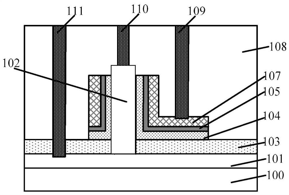
[0032] As mentioned in the background, the performance of the existing fin field effect transistor with surrounding trench gate structure needs to be improved.

[0033] Describe in detail below in conjunction with accompanying drawing, figure 1 It is a structural schematic diagram of a fin field effect transistor with a trench gate surrounding structure.

[0034] Please refer to figure 1 , comprising: a substrate 100; a source-drain doped layer 101 on the substrate 100; a channel column 102 located on the source-drain doped layer 101; The isolation layer 103, the top surface of the isolation layer 103 is lower than the top surface of the channel column 102; the gate structure located on the side wall of the channel column 102, the gate structure includes: a gate dielectric layer 104, located at the gate The work function layer 105 on the dielectric layer 104, and the gate layer 107 on the work function layer 105, part of the gate structure is also located on the surface of t...


PUM

PropertyMeasurementUnit
Thicknessaaaaaaaaaa
Thicknessaaaaaaaaaa

Abstract

The invention discloses a semiconductor structure and a formation method thereof. The method comprises the steps of providing a substrate, wherein the surface of the substrate is provided with a source-drain doping layer; forming a channel column on the surface of part of the source-drain doping layer; forming an initial gate structure on the side wall surface and the top surface of the channel column; forming a first protection layer on the side surface of the initial gate structure; forming a dielectric structure on the substrate, wherein the dielectric structure covers the surface of the first protection layer, and the dielectric structure and the first protection layer are made of different materials; and forming a first conductive plug electrically connected with the source-drain doping layer in the dielectric structure. The semiconductor structure formed by the method is good in performance.

Description

technical field [0001] The invention relates to the technical field of semiconductor manufacturing, in particular to a semiconductor structure and a forming method thereof. Background technique [0002] Fin Field Effect Transistor (Fin FET) is an emerging multi-gate device, which generally includes a fin protruding from the surface of the semiconductor substrate, and a gate structure covering part of the top surface and sidewall of the fin, located at The source and drain doped regions in the fins on both sides of the gate structure. Compared with planar metal-oxide semiconductor field effect transistors, fin field effect transistors have stronger short-channel suppression capability and stronger operating current. [0003] With the further development of semiconductor technology, the size of integrated circuit devices is getting smaller and smaller, and the traditional fin field effect transistor has limitations in further increasing the operating current. Specifically, s...

Claims


Application Information

Patent Timeline
IPC IPC(8): H01L29/78H01L21/336
CPCH01L29/785H01L29/66795
Inventor 周飞
Owner SEMICON MFG INT (SHANGHAI) CORP
Why Eureka
Try Eureka