Adjustable high-optical-efficiency broadband multi-longitudinal-mode Raman microchip laser

An optical efficiency, Raman microchip technology, applied in lasers, laser parts, structures/shapes of optical resonators, etc., can solve problems such as difficulty in achieving high optical efficiency output, limiting output power, etc.

Active Publication Date: 2021-09-07
XIAMEN UNIV
View PDF13 Cites 2 Cited by
  • Summary
  • Abstract
  • Description
  • Claims
  • Application Information

AI Technical Summary

Problems solved by technology

However, the thermal effect caused by the Raman crystal acting as a gain medium and a Raman medium at the same...

Method used


Image

  • Adjustable high-optical-efficiency broadband multi-longitudinal-mode Raman microchip laser
  • Adjustable high-optical-efficiency broadband multi-longitudinal-mode Raman microchip laser
  • Adjustable high-optical-efficiency broadband multi-longitudinal-mode Raman microchip laser

Examples


Embodiment 1

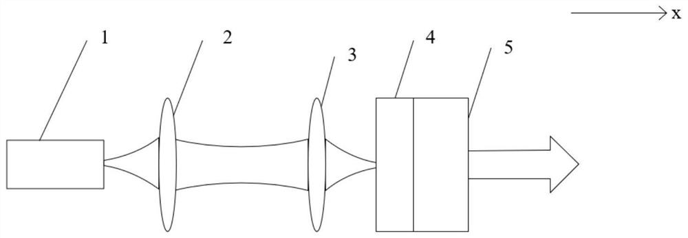
[0069] combine figure 1 As shown, in the present embodiment, the laser crystal 4 selects 1 mm thick 20at% doped Yb:YAG crystal; the Raman crystal 5 selects a-cut YVO with a thickness of 1.5 mm 4 crystals.

[0070] The side of the laser crystal 4 facing the focusing lens 3 is coated with an anti-reflection film for 940nm pump light and a high-reflection film for wavelength 1030-1100nm, which serves as an incident cavity mirror of the laser resonator. The side of the Raman crystal 5 facing the laser crystal 4 is coated with an anti-reflection film for 1030-1100 nm, and the other side is coated with a high-reflection film for 1030-1100 nm, which serves as the output cavity mirror of the laser resonator. The reflectivity of the reflective film to 1030-1100nm laser is greater than 99.5%.

[0071] The pump source 1 is a fiber-coupled quasi-continuous light-emitting diode with a center wavelength of 940nm, the fiber core diameter is 200 μm, the numerical aperture (NA) is 0.22, the ...

Embodiment 2

[0085] combine figure 1As shown, this embodiment is roughly the same as Embodiment 1, and the difference between this embodiment and Embodiment 1 is that this embodiment replaces the Raman crystal 5 with a thickness of 2mm a-cut YVO 4 crystals. The pumping source 1, the collimating lens 2, the focusing lens 3, the laser crystal 4, the optical path and the experimental method are all the same as those in the first embodiment.

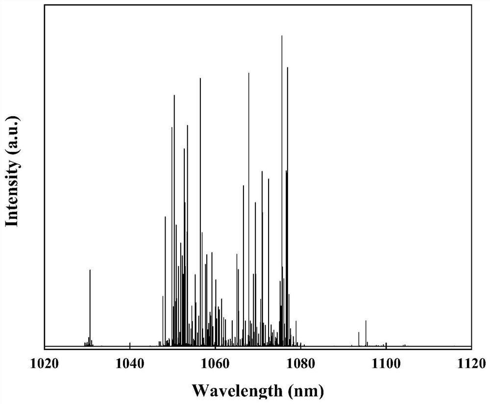
[0086] This embodiment generates 1110nm second-order Raman light on the basis of Embodiment 1, expanding the spectral range of the output laser.

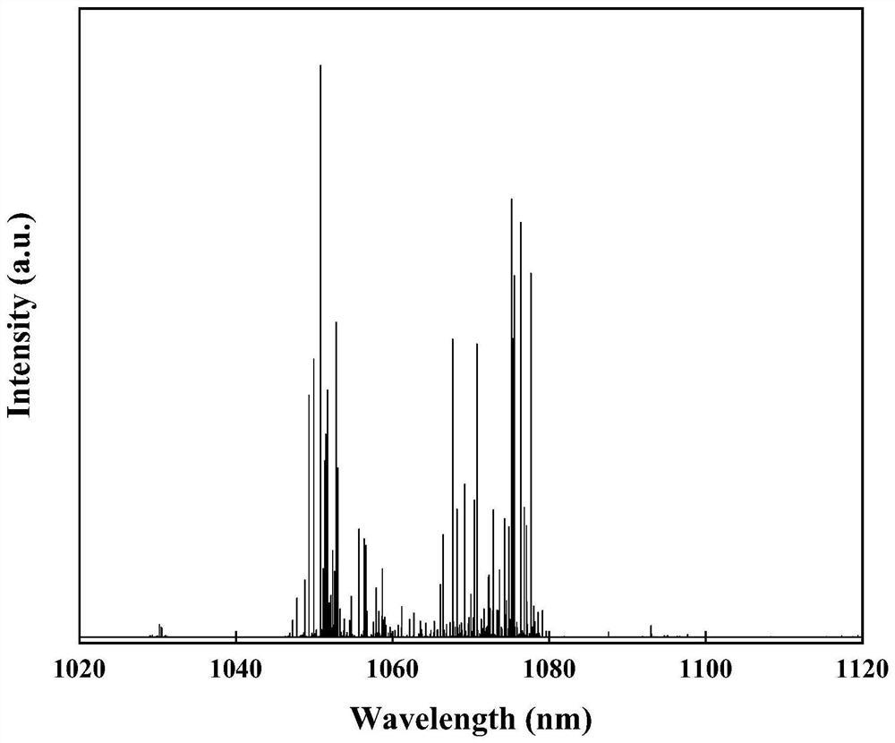
[0087] When Δx=100mm, the radius of the pumping spot shaped by the collimating lens and the focusing lens is 97 μm. As the pump power increases, both the longitudinal mode number and the spectral width of the output laser increase. At pump power P in =35.6W, the obtained broadband multi-longitudinal mode laser spectrum is as follows Figure 5 shown. In the laser spectrum, the 1050nm fundamental frequency...


PUM

PropertyMeasurementUnit
Focal lengthaaaaaaaaaa
Center wavelengthaaaaaaaaaa
Core diameteraaaaaaaaaa

Abstract

The invention discloses an adjustable high-optical-efficiency broadband multi-longitudinal-mode Raman microchip laser. The laser comprises a pumping source, a collimating lens, a focusing lens and a laser resonant cavity which are sequentially arranged along a light path, wherein the pumping source, the collimating lens, the focusing lens and the laser resonant cavity are located on the same horizontal optical axis and are vertically arranged; besides, after being collimated by the collimating lens, pump light emitted by the pumping source enters the focusing lens and is focused on the laser resonant cavity by the focusing lens, and after a pump light spot formed by focusing passes through the laser resonant cavity, broadband multi-longitudinal-mode laser with high optical efficiency is output. The laser is extremely short in cavity length, does not need special design, is simple in structure, is low in cost, facilitates miniaturization and integration of the laser, and is consistent with the development trend of an existing multi-wavelength laser; and according to the scheme, broadband multi-longitudinal-mode laser output can be obtained without inserting additional optical elements inside and outside the laser cavity, and the optical conversion efficiency of the output laser is high.

Description

technical field [0001] The invention relates to the technical field of multi-wavelength lasers, in particular to an adjustable high optical efficiency broadband multi-longitudinal-mode Raman microchip laser. Background technique [0002] Multi-wavelength lasers are now frequently used in laser medicine [1] , optical sensor [2] ,Optical Communication [3] , nonlinear frequency conversion [4] , lidar [5] , generating terahertz waves [6] and other fields. The method of generating multi-wavelength laser is mainly to insert additional optical elements in the laser cavity, and use the emission cross-section of different laser crystals to realize it by adjusting the cavity length and the coating curve of the cavity mirror. Additional inserted optical components, specially designed coatings and laser resonant cavity length increase the cost of the laser and the design complexity is not conducive to popularization. However, the use of the emission line of the laser crystal itse...

Claims


Application Information

Patent Timeline
IPC IPC(8): H01S3/08H01S3/094H01S3/108
CPCH01S3/08086H01S3/094069H01S3/1086
Inventor 董俊刘松
Owner XIAMEN UNIV
Why Eureka
Try Eureka