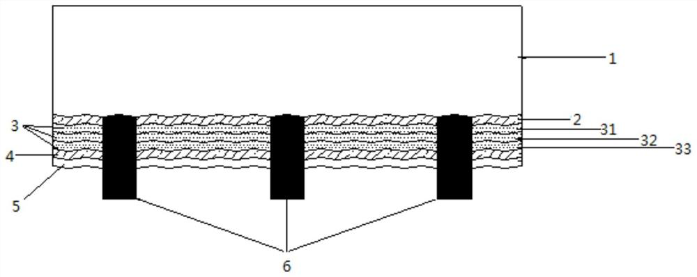
Back film structure of PERC solar cell, preparation method thereof, solar cell and solar cell assembly
A solar cell and back film technology, applied in the field of solar cells, can solve the problems of high production cost of PERC solar cells
- Summary
- Abstract
- Description
- Claims
- Application Information
AI Technical Summary
Problems solved by technology
Method used
Image
Examples
Embodiment 2
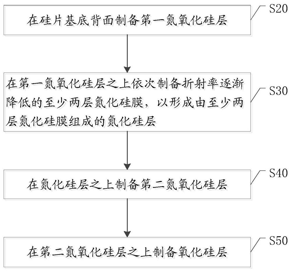
[0068] Please refer to figure 2 , the present invention also provides a preparation method of the back film structure of the PERC solar cell, the preparation method of the back film structure of the PERC solar cell is used to prepare the back film structure of the PERC solar cell of Example 1, the method comprising:
[0069] Step S20, preparing a first silicon oxynitride layer 2 on the back side of the silicon substrate 1;
[0070] In the embodiment of the present invention, the silicon wafer substrate 1 is obtained from a monocrystalline silicon wafer after undergoing texturing, diffusion, SE laser, etching and annealing treatments, and the specific treatment process includes:
[0071] Clean and texture the single crystal silicon wafer, remove the damaged layer on the surface of the silicon wafer, and at the same time make a textured surface on the front surface of the silicon wafer; deposit doping sources on the surface of the single crystal silicon wafer and perform therma...
Embodiment 3
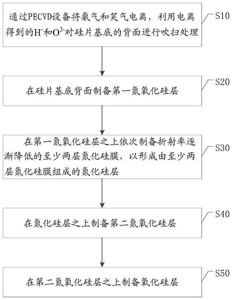
[0089] Please refer to image 3 , on the basis of Embodiment 2, before the step of depositing the first silicon oxynitride layer on the back side of the silicon wafer, it also includes:
[0090] Step S10, using PECVD equipment to ionize ammonia and laughing gas, using the ionized H - and O 2- The backside of the silicon wafer substrate 1 is purged.
[0091] In this step, ammonia and laughing gas are ionized by PECVD equipment, and the H - and O 2- The step of purging the back side of the silicon wafer substrate 1 specifically includes:
[0092] Using PECVD equipment, at a temperature of 410-480°C, an ammonia gas flow of 2500-4000sccm, a laughing gas flow of 2000-5000sccm, a deposition pressure of 900-1600mTor, a radiation power of 3800-5000W, a deposition duty cycle of 2:30-2:60ms, radio frequency Discharge for 120-250s to utilize the ionized H - and O 2- The backside of the silicon wafer substrate is purged.
[0093] In this embodiment, before using PECVD equipment to...
Embodiment 4
[0095] Please refer to Figure 4 , on the basis of Example 3, ammonia gas and laughing gas are ionized by PECVD equipment, and the H - and O 2- After the step of purging the backside of the silicon wafer substrate 1, before the step of preparing the first silicon oxynitride layer 2 on the backside of the silicon wafer substrate 1, it also includes:
[0096] Step S15, using PECVD equipment to ionize the laughing gas, using the ionized O 2- The backside of the silicon wafer substrate 1 is purged.
[0097] In this embodiment, the laughing gas is ionized by PECVD equipment, and the O2- obtained by ionizing the laughing gas is used to further purge the back side of the silicon wafer substrate 1 to saturate the H produced in step S10. + or H 3 o + , can form a neutral or negative electric field, which is beneficial to the subsequent deposition of the first silicon oxynitride layer 2 .
[0098] As an embodiment of the present invention, using O 2- Purging the back of the silic...
PUM
| Property | Measurement | Unit |
|---|---|---|
| thickness | aaaaa | aaaaa |
| thickness | aaaaa | aaaaa |
| thickness | aaaaa | aaaaa |
Abstract
Description
Claims
Application Information


