Power device structure with ESD and preparation method thereof

A technology of power devices and trenches, applied in semiconductor/solid-state device manufacturing, electric solid-state devices, semiconductor devices, etc., can solve problems such as limited electrostatic discharge capacity of Zener diodes, signal distortion, and influence on process planarization, etc., to achieve improvement Effects of ESD leakage performance, area reduction, and manufacturing cost reduction

Active Publication Date: 2021-09-21
SHANGHAI NATLINEAR ELECTRONICS CO LTD +1
View PDF3 Cites 2 Cited by
  • Summary
  • Abstract
  • Description
  • Claims
  • Application Information

AI Technical Summary

Problems solved by technology

However, the electrostatic discharge capability of the Zener diode is limited, which is far lower than that of the parasitic triode, and the Zener diode usually has a capacitance of tens of pF, which is easy to cause signal distortion
In addition, the polysilicon ESD layer is placed on the silicon surface, which affects the planarization of the process; the reverse bias leakage of polysilicon ESD is much higher than that of single crystal PN

Method used


Image

  • Power device structure with ESD and preparation method thereof
  • Power device structure with ESD and preparation method thereof
  • Power device structure with ESD and preparation method thereof

Examples


Embodiment Construction

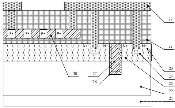
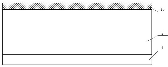
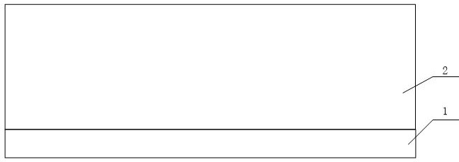
[0031] Embodiments of the present invention are described below through specific examples, and those skilled in the art can easily understand other advantages and effects of the present invention from the content disclosed in this specification. The present invention can also be implemented or applied through other different specific implementation modes, and various modifications or changes can be made to the details in this specification based on different viewpoints and applications without departing from the spirit of the present invention. For example, when describing the embodiments of the present invention in detail, for the convenience of explanation, the cross-sectional view showing the device structure will not be partially enlarged according to the general scale, and the schematic diagram is only an example, which should not limit the protection scope of the present invention. In addition, the three-dimensional space dimensions of length, width and depth should be in...


PUM

PropertyMeasurementUnit
thicknessaaaaaaaaaa
thicknessaaaaaaaaaa
thicknessaaaaaaaaaa

Abstract

The invention provides a power device structure with an ESD and a preparation method thereof. The device comprises an N-type substrate, an N-type epitaxial layer, a first groove, a second groove, a P-type body region, a P-type active region, an N-type active region, a dielectric layer and a metal electrode, wherein the first groove and the second groove are distributed in the N-type epitaxial layer at intervals, a gate oxide layer and polycrystalline silicon ESD are arranged in the first groove, and a P-type doped region is formed in the polycrystalline silicon ESD; a gate oxide layer and a polycrystalline silicon gate are arranged in the second groove; the P-type body region is located in the N-type epitaxial layer between the grooves; the dielectric layer covers the first groove, the second groove and the P-type body region; the hole leading-out region is positioned in the dielectric layer and is electrically contacted with a P-type doped region and a P-type active region of the polycrystalline silicon ESD and an N-type active region in a P-type body region between the first groove and the second groove; and the metal electrode is located on the dielectric layer. The area of the ESD structure can be effectively reduced, the process planarization is facilitated, the device preparation cost is reduced, and the ESD leakage performance is improved.

Description

technical field [0001] The present invention relates to the technical field of semiconductor devices, in particular to a power device, in particular to a structure of a power device with ESD (Electro-Static discharge, electrostatic discharge) and a preparation method thereof. Background technique [0002] Power devices, also known as electronic power devices, are widely used in various consumer electronic equipment and industrial equipment. During the working process of power devices, there is usually a large electric field intensity and current density, which will generate static electricity. If the static electricity cannot be effectively released, it will cause breakdown of the device, shorten the service life of the device, and even cause the device to burn out in severe cases. And cause serious production and life accidents. Therefore, current power devices usually have their own electrostatic protection devices, such as existing trench MOS devices with ESD such as fi...

Claims


Application Information

Patent Timeline
Patent Type & Authority Applications(China)
IPC IPC(8): H01L21/336H01L27/02H01L29/78
CPCH01L27/0255H01L29/7808H01L29/7813H01L29/66734
Inventor 许剑吴春达蒋小强霍晓强
Owner SHANGHAI NATLINEAR ELECTRONICS CO LTD
Why Eureka
Try Eureka