

Three-dimensional SRRs-based metamaterial microstrip antenna and manufacturing method thereof
A technology of microstrip antenna and manufacturing method, which is applied in the direction of antenna, radiating element structure, electrical components, etc., to achieve the effects of excellent performance, size reduction, and high reliability
- Summary
- Abstract
- Description
- Claims
- Application Information
AI Technical Summary
Problems solved by technology
Method used
Image


Examples
Embodiment 1
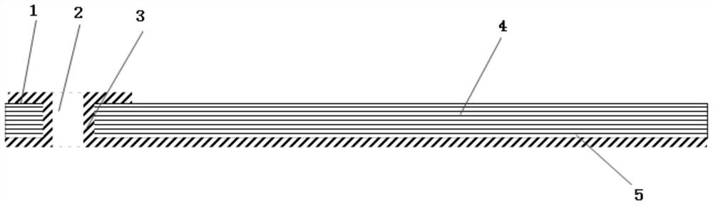
[0054] as attached figure 2 and Figure 4 As shown, the microstrip antenna in this embodiment 1 includes three layers of inner layer dielectric RT6010 (thickness 0.254mm) 4, two layers of 2929 bonding material 11, antenna pattern 1, feed hole 2 for connector installation, and feed hole The metallized hole wall 3, the bottom microwave ground 5, and the three-dimensional SRRs graphics.
[0055] The three-dimensional SRRs pattern includes: side SRR pattern 6 (composed of metallized hole walls and conductive paste), SRR pattern 9 on the upper layer of the inner layer board and SRR pattern 10 on the lower layer of the inner layer board. Metal plug hole 7 (made up of metal plug hole wall 13 and conductive paste 12) is arranged between two rows of three-dimensional SRRs pattern. The SRR pattern structure size of embodiment 1 is shown in table 1 below, wherein a is the length of dielectric unit, b is the width of the dielectric unit, c is the height of the dielectric unit, L is the...
Embodiment 2
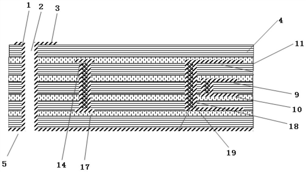
[0061] such as 3 and Figure 5 As shown, the microstrip antenna in this embodiment 2 includes five layers of inner dielectric layer RT6010 (thickness 0.254mm) 4, four layers of 2929 bonding material 11, antenna pattern 1, feed hole 2 for connector installation, feed The metallized hole wall of the hole 3, the microwave ground of the bottom layer 5, and the three-dimensional nested SRRs pattern.
[0062] Three-dimensional nested SRRs pattern: the inner layer SRRs pattern is similar to Embodiment 1, including side SRR pattern 6 (composed of metallized hole wall and conductive paste), upper layer SRR pattern 9 of inner layer board and lower layer SRR pattern 10 of inner layer board , the outer layer nested SRRs pattern includes the outer layer side SRR pattern 15 (composed of the metallized hole wall 1 and the conductive paste 2), the upper layer SRRs pattern 14 of the outer layer board and the lower layer SRRs pattern 17 of the outer layer board. A metal plug hole 16 (composed ...
PUM
| Property | Measurement | Unit |
|---|---|---|
| thickness | aaaaa | aaaaa |
| width | aaaaa | aaaaa |
| thickness | aaaaa | aaaaa |
Abstract
Description
Claims
Application Information