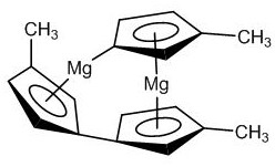
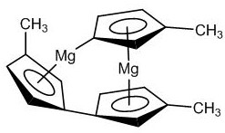
Organic magnesium compound and electronic device
A technology for electronic devices and compounds, applied in magnesium organic compounds, electrical components, semiconductor devices, etc., can solve the problems of uneven magnesium doping concentration in chips, inability to meet requirements, and only suitable for magnesium compounds, and improve the stability of production processes. The effect of improving the production rate of gallium and the uniform distribution of magnesium components
- Summary
- Abstract
- Description
- Claims
- Application Information
AI Technical Summary
Problems solved by technology
Method used
Image
Examples
preparation example Construction
[0025] The preparation process of the organic magnesium compound represented by the structural formula (1) is as follows:
[0026] In an anhydrous anhydress oxygenless glove box, in the quartz synthetic column with a heating wire, high-pure magnesium films were added to the baffle in the synthetic column, and the synthetic column was placed vertically; There is a 500 mL band rotor champion, and the funnel is added to 500 ml of methylcyclopentadiene monomer. The upper port is connected to the argon cylinder; below the synthetic column, 2,000 ml of two flasks, the flask remaining The interface is connected to the serpentine condenser, the coolant sets 32 ° C, the condenser upper mouth is connected to the exhaust gas absorbing device; the synthesis apparatus in the 5 l / min, the nitrogen in the synthesis apparatus is replaced, and the time is 30 min, and the purge is complete. After adjusting the airflow to the bubble device, the foam is bubbles at a speed per second; the heating wi...
Embodiment 1
[0042] An epitaxial sheet of the light-emitting diode was prepared as a dopant using the organic magnesium compound as shown in structure formula (1):
[0043] 1) Place the sapphire substrate into the carrier disk in the MOCVD reaction chamber, grow 25 nm buffer layer under temperature 540 ° C, growth pressure 300 TORR conditions, wherein the buffer layer is a low temperature GaN buffer layer, and the GA source required for growth TMG source (trimethyl gallium), growth atmosphere is h 2 Atmosphere;
[0044] 2) On the buffer layer, a non-intentional doped nitride layer having a temperature of 2.5 μm is grown at a temperature of 1080 ° C, a growth pressure 200 TORR, wherein the non-intentional doped nitride layer is non-intentionally doped GaN layer, the desired GA source is TMG source, the growth atmosphere is h 2 Atmosphere;
[0045] 3) On the non-intentionally doped nitride layer, the N-type nitride layer of 2.5 μm is grown under temperature 1060 ° C, the growth pressure 200 TORR...
PUM
| Property | Measurement | Unit |
|---|---|---|
| melting point | aaaaa | aaaaa |
| melting point | aaaaa | aaaaa |
Abstract
Description
Claims
Application Information
 - R&D
- Intellectual Property
- Life Sciences
- Materials
- Tech Scout
- Unparalleled Data Quality
- Higher Quality Content
- 60% Fewer Hallucinations
Browse by: Latest US Patents, China's latest patents, Technical Efficacy Thesaurus, Application Domain, Technology Topic, Popular Technical Reports.
© 2025 PatSnap. All rights reserved.Legal|Privacy policy|Modern Slavery Act Transparency Statement|Sitemap|About US| Contact US: help@patsnap.com


