Method for preparing two-dimensional precious metal micro-nano pattern large-scale array

A technology of micro-nano patterns and precious metals, which is applied in the direction of metal material coating process, liquid chemical plating, coating, etc., to achieve the effect of less process, high utilization rate and low loss

Active Publication Date: 2021-10-01
ZHENGZHOU UNIV
View PDF5 Cites 0 Cited by
  • Summary
  • Abstract
  • Description
  • Claims
  • Application Information

AI Technical Summary

Problems solved by technology

In order to control the position of polymer crystals, the anti-etching layer needs to be completely

Method used


Image

  • Method for preparing two-dimensional precious metal micro-nano pattern large-scale array
  • Method for preparing two-dimensional precious metal micro-nano pattern large-scale array
  • Method for preparing two-dimensional precious metal micro-nano pattern large-scale array

Examples


Embodiment 1

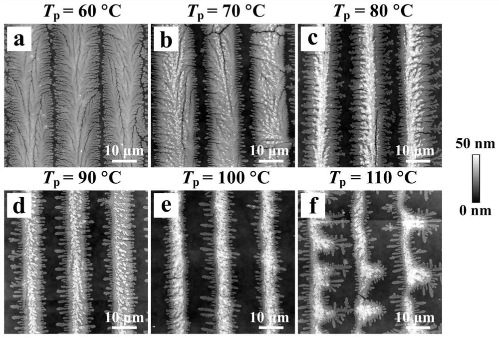
[0044] Embodiment 1 Hot-pressing temperature is to PEO -b- Effects of P2VP crystallographic pattern arrays

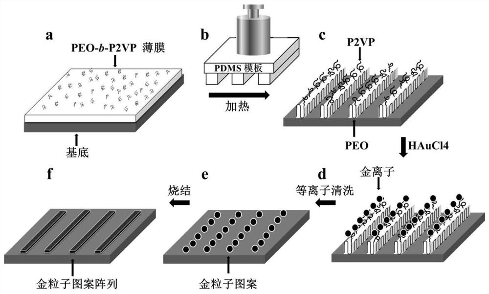
[0045] Preparation of PEO by Spin Coating -b- P2VP ultra-thin film: First, wrap the sample bottle and cap with a specification of 6mL with aluminum foil and blow it with high-purity nitrogen; then PEO -b- P2VP (4000-2000g / mol) and toluene (analytically pure) were formulated into a solution with a concentration of 0.5wt-%, and then the solution was placed on a hot stage at 105°C for 3 hours, and stirred continuously until the solute was fully dissolved. Afterwards, place the clean silicon wafer in a spin coater (model: KW-4A, purchased from the Institute of Microelectronics, Chinese Academy of Sciences), and take 16 μL of PEO -b- The P2VP solution is placed in the center of the silicon wafer, and spin-coated on the homogenizer for 120s by centrifugal force to obtain PEO with a film thickness of 14.5nm. -b- P2VP ultrathin film, such as figure 1 a.

[0046] Then the u...

Embodiment 2

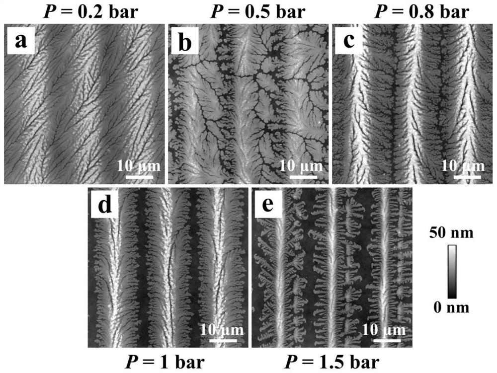
[0049] Embodiment 2 hot pressing pressure is to PEO -b- Effects of P2VP crystallographic pattern arrays

[0050] PEO with a film thickness of 14.5nm -b- The P2VP ultra-thin film is placed on a hot stage and heated to a hot pressing temperature of 90°C ( T p ) for 10 min; place the PDMS soft template in the PEO -b- On the P2VP ultra-thin film, after holding the pressure for 10s so that the material is squeezed into the cavity layer of the PDMS soft template; the hot-pressed PEO- b -The P2VP sample was placed on an aluminum plate and quenched to room temperature (demolding temperature); then the pressure was released and the PDMS soft template was removed from the PEO -b- Remove the P2VP ultrathin film.

[0051] Depend on image 3 The results shown in a-e show that there is no material on the silicon substrate hot-pressed by the protrusions of the soft template. And with the increase of the hot pressing pressure, the PEO in the hot pressing film -b- The width of P2VP lam...

Embodiment 3

[0052] The heating rate of embodiment 3 selective melting is to PEO -b- Effects of P2VP crystallographic pattern arrays

[0053] Under the protection of nitrogen, the hot pressing conditions are T p = 90°C, P = 1 bar of PEO -b- The P2VP hot-pressed film was placed at 24°C for isothermal crystallization for 24 h to obtain striped initial crystals as figure 2 shown in d; then at different heating rates ( V ) 1°C / min, 2°C / min and 5°C / min from 24°C to partial melting temperature ( T s ) at 47°C for 3 minutes; then lower the temperature to 42°C for 3 minutes at a cooling rate of 5°C / min for isothermal crystallization; quickly take out the sample and place it on an aluminum plate to cool to room temperature.

[0054] Depend on Figure 4 The results shown in a-c show that with the increase of the heating rate of selective melting, PEO -b- The nucleation density of P2VP crystals decreases, and they are concentrated in the center of the strip-shaped template, arranged in a ...


PUM

PropertyMeasurementUnit
Film thicknessaaaaaaaaaa
Electric currentaaaaaaaaaa

Abstract

The invention belongs to the technical field of micro-nano processing, and particularly relates to a method for preparing a two-dimensional precious metal micro-nano pattern large-scale array. According to the method, the thin film is prepared by spin coating of a polyoxyethylene-b-poly (2-vinylpyridine) (PEO-b-P2VP) solution. A PDMS soft template is used for hot-pressing a film, and crystal pattern arrays with different widths can be obtained by changing the hot-pressing temperature and the hot-pressing pressure. The size and position of the crystal pattern array can be regulated and controlled through selective melting and dissolving, and finally, a proper precursor is selected to be subjected to a complexation reaction with P2VP to obtain the precious metal pattern array. According to the construction method disclosed by the invention, the size and the position of the precious metal pattern are regulated and controlled on the micro-nano scale. The constructed precious metal pattern array has good conductivity, and the application of the precious metal pattern array in the fields of sensors, energy and the like is expected to be expanded.

Description

technical field [0001] The invention belongs to the technical field of micro-nano processing, and in particular relates to a method for preparing a large-scale array of two-dimensional noble metal micro-nano patterns. Background technique [0002] Noble metal micro-nano patterns have the characteristics of high electrical conductivity, surface plasmon resonance effect, and excellent catalytic activity, and are increasingly widely used in the research and application of nano-optoelectronic devices, surface-enhanced spectroscopy, and biosensors. Compared with the disordered micro-nano noble metal pattern, the quantum effect of the array pattern is more prominent, so it shows more excellent performance. At present, most solar cells are covered with a layer of noble metal pattern arrays on the surface by spin coating or deposition methods. Patterned arrays are less reported. [0003] Although two-dimensional micro-nano noble metal patterns can be obtained by the block copolyme...

Claims


Application Information

Patent Timeline
IPC IPC(8): C08J7/12C23C18/18C23C18/42C08L87/00
CPCC08J7/12C23C18/1886C23C18/42C08J2387/00
Inventor 陈静波张彬王兴昱王冰花
Owner ZHENGZHOU UNIV
Why Eureka
Try Eureka