Indium composite microcrystal bump texture
A bump and microcrystalline technology is applied in the field of indium composite microcrystalline bump texture to achieve the effects of improving connection reliability, good heat dissipation performance and strong applicability
- Summary
- Abstract
- Description
- Claims
- Application Information
AI Technical Summary
Problems solved by technology
Method used
Image
Examples
Embodiment 1
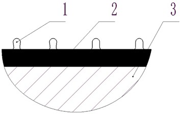
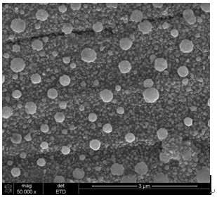
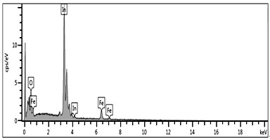
[0016] figure 1 It is a schematic structural diagram of the indium composite microcrystalline bump texture in Example 1 of the present invention, figure 2 is the scanning electron microscope image of the indium composite microcrystalline bump texture sample of Example 1 of the present invention, image 3 For embodiment 1 of the present invention figure 2 The energy spectrum corresponding to the indium composite microcrystalline bump texture sample in the figure, 1 is the bump crystallite, 2 is the composite material layer, and 3 is the part.
[0017] The indium composite microcrystalline bump texture of the present invention is characterized in that: on the surface of the part, a structure containing more than 60% (wt%) of indium and more than 8% (wt%) of iron and more than 70% (wt%) of indium and iron together is set on the surface of the part. ) composite material layer, on the surface of the composite material layer, there are many bump crystallites, the top of each bum...
PUM
| Property | Measurement | Unit |
|---|---|---|
| diameter | aaaaa | aaaaa |
| diameter | aaaaa | aaaaa |
| height | aaaaa | aaaaa |
Abstract
Description
Claims
Application Information


