UVLED epitaxial structure, preparation method thereof, and UVLED chip

An epitaxial structure and chip technology, which is applied in electrical components, nanotechnology, circuits, etc., can solve the problems of weakening quantum dot effect, low luminous efficiency of UVLED, and decreased luminous efficiency, and achieve high luminous efficiency and enhanced quantum dot effect. Effect

Active Publication Date: 2021-10-26
EPITOP PHOTOELECTRIC TECH
View PDF7 Cites 0 Cited by
  • Summary
  • Abstract
  • Description
  • Claims
  • Application Information

AI Technical Summary

Problems solved by technology

[0003] Ultraviolet (UV) radiation is divided into A-band (320-400nm), B-band (275-320nm) and C-band (200-275nm), And they are called UVA, UVB and UVC respectively. The market share of UVA LED chips with wavelengths from 360nm to 400nm is getting higher and higher, and they have important applications in lighting, sterilization, medical treatment, printing, testing, photocuring, insect trapping and other fields. value, but compared with blue-green light as the three primary colors, the luminous efficiency of ultraviolet LED is low, and as the wavelength becomes shorter, the In composition decreases, the quantum dot effect becomes weaker, and the difference in the forbidden band width of the well barrier becomes smaller , the luminous efficiency drops more obviously
[0004]So how to solve the low luminous efficiency of UV LED is an urgent technical problem in the industry

Method used


Image

  • UVLED epitaxial structure, preparation method thereof, and UVLED chip
  • UVLED epitaxial structure, preparation method thereof, and UVLED chip
  • UVLED epitaxial structure, preparation method thereof, and UVLED chip

Examples


preparation example Construction

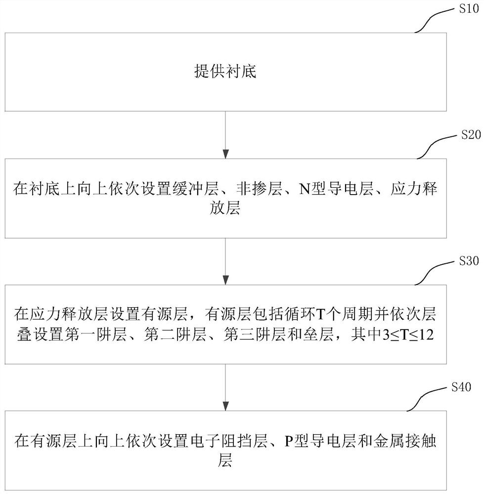
[0076] The present invention also provides a method for preparing a UVLED epitaxial structure, which is used for preparing the above-mentioned UVLED epitaxial structure. refer to image 3 Shown is the flow chart of the preparation method of the UVLED epitaxial structure provided in the first embodiment to the fifth embodiment, and the preparation method includes:

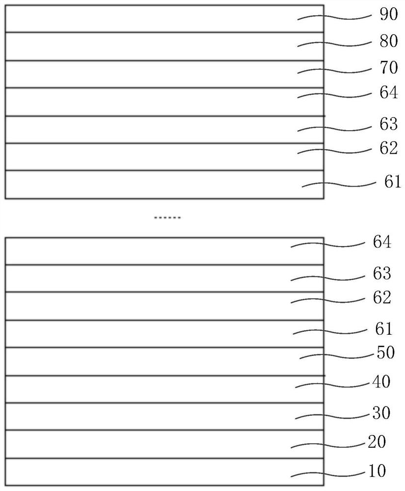
[0077] S10, provide the substrate 10; put the substrate 10 into a metal organic compound vapor phase epitaxy deposition equipment

[0078] S20, a buffer layer 20, a non-doped layer 30, an N-type conductive layer 40, and a stress release layer 50 are sequentially arranged upward on the substrate 10;

[0079] In a possible implementation manner, the growth buffer layer 20 , the undoped layer 30 , the N-type conductive layer 40 , and the stress release layer 50 are sequentially deposited on the substrate 10 .

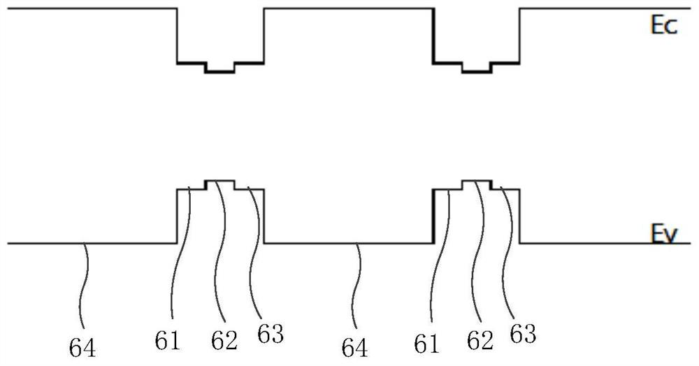
[0080] S30. Repeatedly arrange T active layers 60 on the stress release layer 50. The active layer 60 inclu...

Embodiment 1

[0086] The active layer 60 is grown for 5 cycles in the environment of high-purity hydrogen H2, high-purity N2 or high-purity H2 / N2 mixed gas as the carrier gas, that is, the first well layer 61, the second well layer 62, the third well layer 63 and barrier layer 64 are stacked repeatedly for 5 layers.

[0087] In a possible implementation manner, the flow rate of triethylgallium (TEGa) can be set to 120 sccm, the flow rate of trimethylindium (TMIn) can be set to 200 sccm, and the flow rate of trimethylaluminum (TMAl) Set to 10 sccm, under the conditions of 200 Torr pressure and growth temperature of 840°C, grow for 2min to 5min, control the growth thickness of the first well layer 61 to 1.0nm, and the first well layer 61 is made of Al x1 In y1 Ga (1-x1-y1) N layers, where x1 can be 0.02 and y1 can be 0.025.

[0088] In a possible implementation manner, in S30, the flow of triethylgallium (TEGa) can be set to 120 sccm, the flow of trimethyl indium (TMIn) can be set to 100 s...

Embodiment 2

[0095] The active layer 60 is grown for 5 cycles in the environment of high-purity hydrogen H2, high-purity N2 or high-purity H2 / N2 mixed gas as the carrier gas, that is, the first well layer 61, the second well layer 62, the third well layer 63 and barrier layer 64 are stacked repeatedly for 5 layers.

[0096] The flow rate of trimethylindium (TMIn) in the first well layer 61 is set to 100 sccm, the flow rate of trimethylaluminum (TMAl) is set to 15 sccm, under the conditions of a pressure of 200 Torr and a growth temperature of 840° C., grow for 2 minutes to 5 minutes, control the growth thickness of the first well layer 61 to be 1.0 nm, and the first well layer 61 is made of Al x1 In y1 Ga (1-x1-y1) N, where x1 can be 0.025 and y1 can be 0.015;

[0097] The flow rate of trimethylindium (TMIn) in the third well layer 63 is set to 100 sccm, the flow rate of trimethylaluminum (TMAl) is set to 15 sccm, under the conditions of a pressure of 200 Torr and a growth temperature o...


PUM

PropertyMeasurementUnit
thicknessaaaaaaaaaa
thicknessaaaaaaaaaa
thicknessaaaaaaaaaa

Abstract

The invention provides a UVLED epitaxial structure, a preparation method thereof, and a UVLED chip, and the UVLED epitaxial structure comprises a substrate, a buffer layer, a non-doped layer, an N-type conductive layer, a stress release layer, an active layer, an electron blocking layer, a P-type conductive layer, and a metal contact layer which are sequentially stacked. The active layer comprises a first well layer, a second well layer, a third well layer and a barrier layer which are sequentially stacked in T periods, and T is larger than or equal to 3 and smaller than or equal to 12. The UVLED epitaxial structure, the preparation method thereof and the UVLED chip provided by the invention are used for at least improving the luminous efficiency of a UVALED.

Description

technical field [0001] The invention relates to the technical field of semiconductor optoelectronics, in particular to a UVLED epitaxial structure, a preparation method thereof, and a UVLED chip. Background technique [0002] With the continuous development of science and technology, various LEDs (Light Emitting Diodes, light emitting diodes) can directly convert electrical energy into light energy, and have been widely used in people's daily life, work and industry. The UVLED epitaxial structure is a substrate structure that can be heated to an appropriate temperature. Its material is the cornerstone of the development of semiconductor lighting industry technology. UVLED chips are generally formed by further processing LED epitaxial wafers. [0003] Ultraviolet (UV) radiation is divided into A-band (320-400nm), B-band (275-320nm) and C-band (200-275nm), which are called UVA, UVB and UVC respectively. The market share of 400nm segment UVA LED chips is getting higher and hig...

Claims


Application Information

Patent Timeline
Patent Type & Authority Applications(China)
IPC IPC(8): H01L33/06H01L33/32H01L33/00B82Y30/00B82Y40/00
CPCH01L33/06H01L33/325H01L33/007H01L33/0075B82Y30/00B82Y40/00
Inventor 蔡武康建陈向东
Owner EPITOP PHOTOELECTRIC TECH
Why Eureka
Try Eureka