Indium gallium bismuth nitride material, laser and detector using the material and preparation method

A technology of indium gallium nitride and lasers, which is applied in the field of semiconductor photoelectric material preparation, can solve the problems of threading dislocations, and achieve the effects of easy growth, easy control, simple structure and operation process

Active Publication Date: 2019-11-29
CHAOJING TECH BEIJING CO LTD
View PDF4 Cites 0 Cited by
  • Summary
  • Abstract
  • Description
  • Claims
  • Application Information

AI Technical Summary

Problems solved by technology

In addition, InGaN alloys have a high density of structural defects, such as: threading dislocations, stacking faults

Method used


Image

  • Indium gallium bismuth nitride material, laser and detector using the material and preparation method
  • Indium gallium bismuth nitride material, laser and detector using the material and preparation method
  • Indium gallium bismuth nitride material, laser and detector using the material and preparation method

Examples


Embodiment 1

[0074] Example 1: InGaNBi near-infrared laser

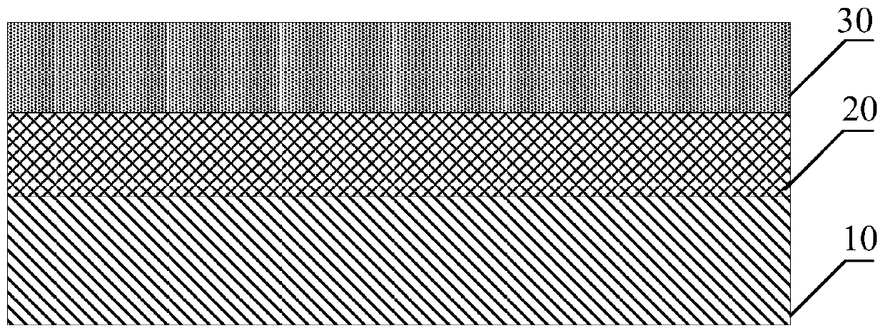
[0075] Using molecular beam epitaxy (MBE) or metal organic vapor deposition (MOCVD) epitaxial growth tools, epitaxially grow the InP buffer layer on the InP substrate (substrate) or auxiliary substrate (template);

[0076] Epitaxial growth of In on the InP buffer layer y Ga 1-y N 1-x Bi x Thin films and heterojunction materials.

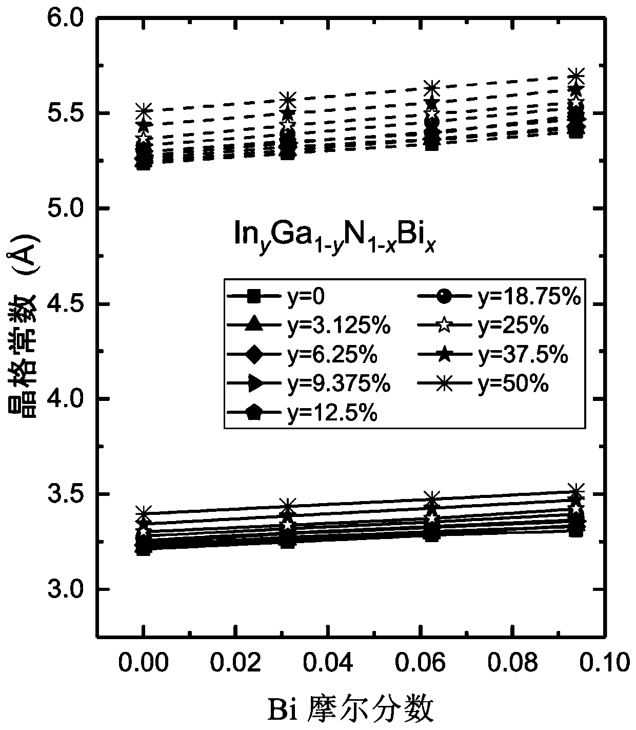
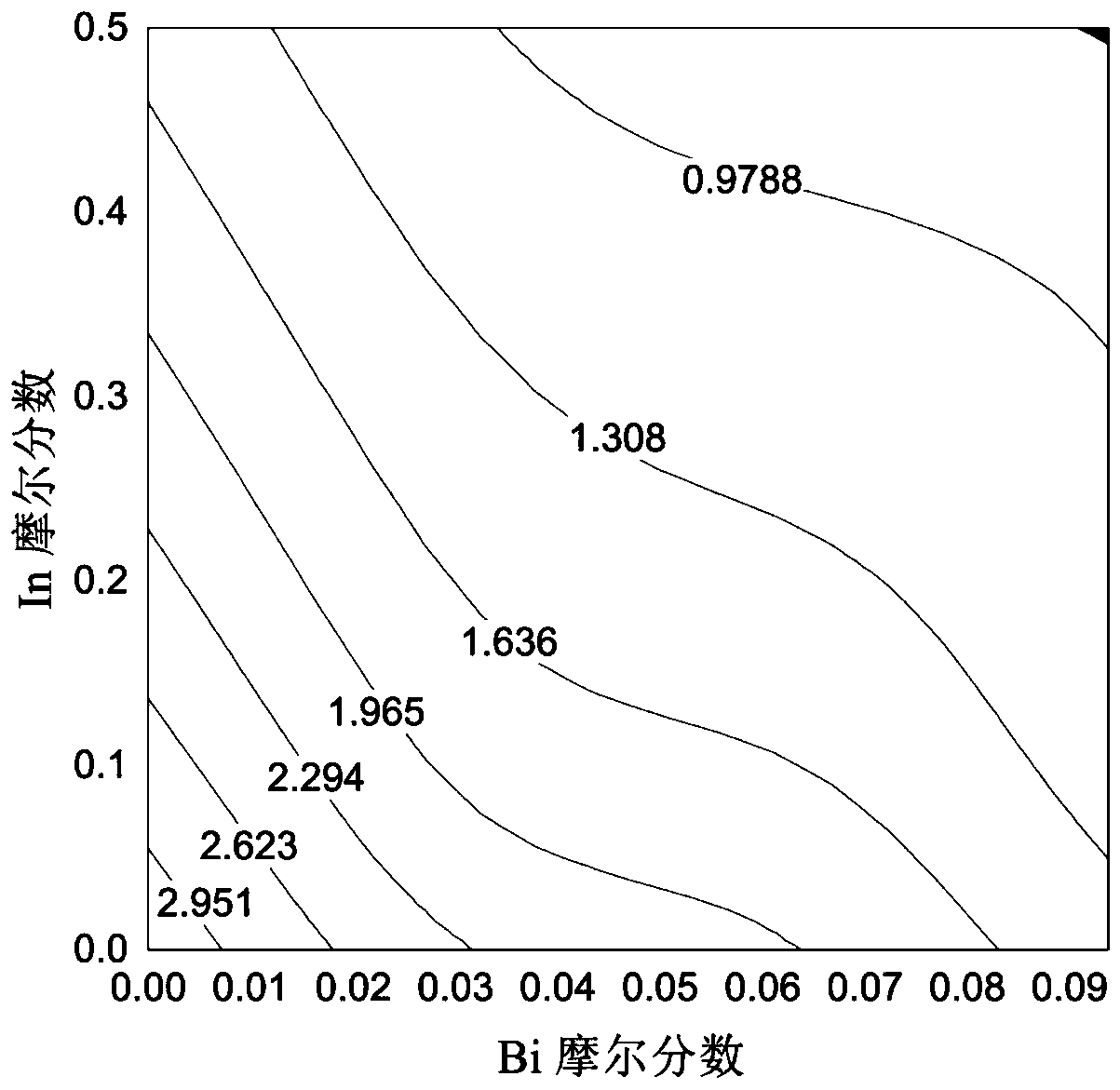
[0077] By controlling the concentration of doped In atoms and Bi atoms, the In y Ga 1-y N 1-x Bi x The band gap of the material, the wavelength range can cover visible light to near infrared.

[0078] Figure 4 In the embodiment 1 of the present application contains In y Ga 1-y N 1-x Bi x Schematic diagram of the structure of a near-infrared laser. In this example, the In of sphalerite structure y Ga 1-y N 1-x Bi xThe material has a forbidden band width of 0.651eV when the In component is 50% and the Bi component is 9.375%, and the corresponding wavelength is 1.9 μm, which is located i...

Embodiment 2

[0097] Example 2: InGaNBi near-infrared detector

[0098] Figure 5 is according to an embodiment of the present application containing In y Ga 1-y N 1-x Bi x Schematic diagram of the near-infrared detector structure. In this example, the In of sphalerite structure y Ga 1-y N 1-x Bi x The material has a forbidden band width of 0.651eV when the In component is 50% and the Bi component is 9.375%, and the corresponding wavelength is 1.9 μm, which is located in the near-infrared band. The specific structure of the near-infrared detector prepared with this material is described as follows:

[0099] Such as Figure 5 As shown, the near-infrared detector includes in order from bottom to top: an InP substrate layer, an N-type InP doped layer, a P-type InGaNBi absorption region, and a P-type InP doped layer,

[0100] Wherein, a passivation layer is deposited on the outer surface of the N-type InP doped layer, the P-type InGaNBi absorption region, and the P-type InP doped lay...


PUM


Abstract

The application discloses an indium gallium nitrogen bismuth material, a laser and a detector using the material, and a preparation method of the material, relating to a semiconductor material. The indium gallium nitrogen bismuth material comprises a substrate layer, a buffer layer, and the indium gallium nitrogen bismuth material, wherein the indium gallium nitrogen bismuth material is formed bysimultaneously incorporating indium atoms and bismuth atoms into GaN alloy, which can adjust the lattice constant and electronic properties of the matrix to improve the luminous efficiency. The application effectively adjusts the forbidden band width of the GaN material by adjusting the incorporated concentration of the indium atoms and germanium atoms, which realizes coverage from the visible light to the near-infrared band and is applied to the optoelectronic device. The co-doping of indium atoms and germanium atoms makes the material easier to grow and more stable. The application can be grown by various methods such as conventional molecular beam epitaxy and metal organic chemical vapor deposition, and the structure and operation process are simple and easy to control.

Description

technical field [0001] The application relates to the field of semiconductor optoelectronic material preparation, in particular to an indium gallium bismuth nitride material, a laser and a detector using the material and a preparation method. Background technique [0002] In recent years, InGaN alloys and InGaN / GaN quantum wells have attracted widespread attention because they can be used to develop high-efficiency light-emitting diodes (LEDs), laser diodes, and solar cells. However, due to the biaxial compressive stress caused by the InGaN layer, the commonly used [0001] direction InGaN / GaN quantum well has a strong built-in electric field. The built-in electric field will cause the quantum well to red-shift the luminescence band, and reduce the resonance intensity of the electron-hole pair at the same time. In addition, InGaN alloys have a high density of structural defects, such as threading dislocations and stacking faults. These structural defects are largely related ...

Claims


Application Information

Patent Timeline
Patent Type & Authority Patents(China)
IPC IPC(8): H01L31/0304H01L31/109H01L31/18H01S5/343
CPCH01L31/03048H01L31/109H01L31/1848H01S5/343H01S5/34346Y02P70/50
Inventor 芦鹏飞张凡梁丹王庶民张丽
Owner CHAOJING TECH BEIJING CO LTD
Why Eureka
Try Eureka