
Local passivation contact IBC battery structure and preparation method thereof
A local, passivation film technology, applied in the field of solar cells, which can solve problems such as optical loss
Patent Information
- Authority / Receiving Office
- CN · China
- Patent Type
- Applications(China)
- Current Assignee / Owner
- Publication Date
- 2021-11-05
Smart Images

Figure 1 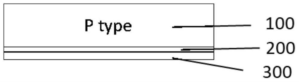
Figure 2 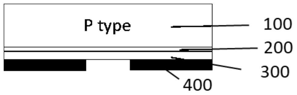
Figure 3
Abstract
Description
technical field
[0001] The invention relates to the technical field of solar cells, in particular to an IBC solar cell with partial back passivation contact and a preparation method thereof. Background technique
[0002] A solar cell is a semiconductor device that can convert solar energy into electrical energy. Lower cost of electricity has always been the goal pursued by the solar cell industry. At present, the mainstream product in the industry is the P-type PERC crystalline silicon solar cell, and its efficiency is already close to the theoretical level of this structure, and there is little room for further efficiency improvement. The battery technology is simple, and the p+ doped region contact electrodes and the n+ doped region contact electrodes are respectively located on the front and back sides of the battery sheet. The front of the battery is the light-receiving surface, and the coverage of the metal contact electrodes on the front will inevitably cause a part o...
Examples
Embodiment
[0024] An IBC solar cell with partial back passivation contact, comprising a P-type crystalline silicon substrate 100, the back surface of the P-type crystalline silicon substrate 100 sequentially includes tunnel oxide layers 200, alternately arranged back surface n+ doped The impurity layer 300 and the p+ doped region 101 at the groove on the back surface, the passivation film 503 on the back surface, and the metal electrode on the back surface; Front surface passivation film 501 and anti-reflection film 502;
[0025] The antireflection film 502 includes SiO 2 and / or Al 2 o 3 dielectric film and SiNx dielectric film or SiOxNy, the SiO 2 The thickness of the dielectric film is 1-5nm, and the Al 2 o 3 The thickness of the dielectric film is 2-20nm, the thickness of the SiNx dielectric film is 40-100nm, and the thickness of the SiOxNy dielectric film is 40-100nm;
[0026] The tunnel oxide layer 200 and the n+ doped layer 300 constitute the emitter region on the back surfac...