Superconducting integrated circuit layout optimization method and device, storage medium, and terminal

A layout optimization, integrated circuit technology, applied in the direction of electrical digital data processing, special data processing applications, instruments, etc., can solve the problem of spending a lot of time, affecting the chip iteration cycle, and unable to meet the requirements of large-scale automatic design of superconducting integrated circuits and other problems to achieve the effect of improving the calculation effect and optimizing the layout results

Active Publication Date: 2021-11-09
SHANGHAI INST OF MICROSYSTEM & INFORMATION TECH CHINESE ACAD OF SCI
View PDF7 Cites 0 Cited by
  • Summary
  • Abstract
  • Description
  • Claims
  • Application Information

AI Technical Summary

Problems solved by technology

[0005] The technical problem to be solved by the present invention is that existing electronic design automation tools cannot meet the requirements of large-scale automatic design of superconducting integrated circuits such as SFQ circuits, and manual layout optimization will take a huge amount of time, seriously affecting the iteration cycle of the chip

Method used


Image

  • Superconducting integrated circuit layout optimization method and device, storage medium, and terminal
  • Superconducting integrated circuit layout optimization method and device, storage medium, and terminal
  • Superconducting integrated circuit layout optimization method and device, storage medium, and terminal

Examples


Embodiment 1

[0066] In order to solve the technical problems existing in the prior art, an embodiment of the present invention provides a method for optimizing the layout of a superconducting integrated circuit.

[0067] figure 1 It shows a schematic flow chart of a superconducting integrated circuit layout optimization method according to an embodiment of the present invention; refer to figure 1 As shown, the method for optimizing the layout of a superconducting integrated circuit in the embodiment of the present invention includes the following steps.

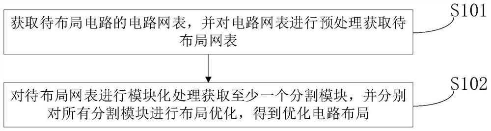
[0068] Step S101, obtaining a circuit netlist of a circuit to be placed, and performing preprocessing on the circuit netlist to obtain a netlist to be placed.

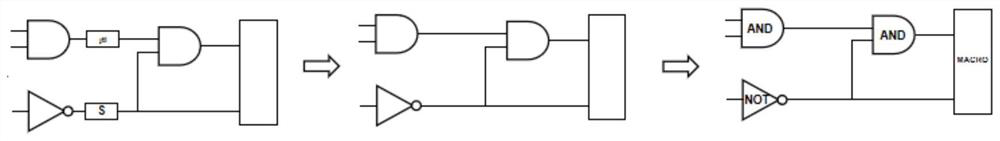
[0069] Specifically, the circuit netlist after logic synthesis of the circuit to be placed is obtained, and then the circuit netlist is preprocessed to obtain the netlist to be placed. figure 2 It shows a schematic diagram of the effect of preprocessing the circuit netlist in E...

Embodiment 2

[0091] In order to solve the technical problems existing in the prior art, an embodiment of the present invention provides a superconducting integrated circuit layout optimization device.

[0092] Figure 9 It shows a schematic structural diagram of a superconducting integrated circuit layout optimization device according to Embodiment 2 of the present invention; refer to Figure 9 As shown, the device for optimizing the layout of a superconducting integrated circuit according to the embodiment of the present invention includes a preprocessing mechanism and an optimization mechanism.

[0093] The preprocessing mechanism is used to obtain the circuit netlist of the circuit to be identified, and preprocess the circuit netlist to obtain the netlist to be laid out;

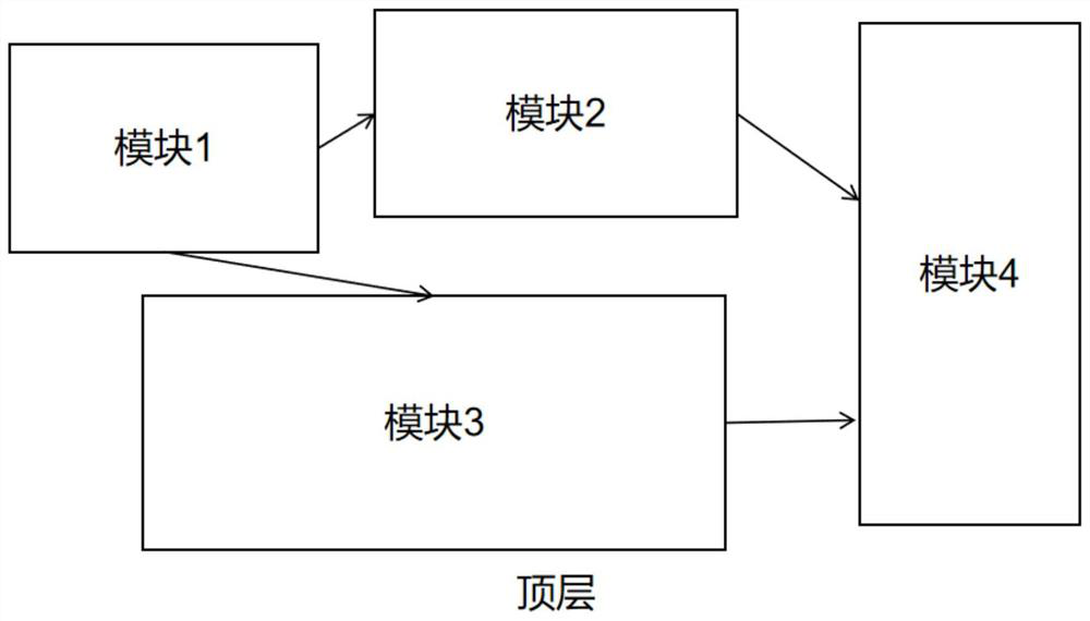
[0094] The optimization mechanism performs modular processing on the layout netlist to obtain at least one segmentation module, and performs global layout optimization on all segmentation modules respectively to obta...

Embodiment 3

[0103] In order to solve the above-mentioned technical problems existing in the prior art, an embodiment of the present invention also provides a storage medium, which stores a computer program, and when the computer program is executed by a processor, it can realize Embodiment 1 Superconducting Integrated Circuit Layout Optimization Method All steps in .

[0104] The specific steps of the superconducting integrated circuit layout optimization method and the beneficial effects obtained by applying the readable storage medium provided by the embodiment of the present invention are the same as those of the first embodiment, and will not be repeated here.

[0105] It should be noted that the storage medium includes various media capable of storing program codes such as ROM, RAM, magnetic disk or optical disk.


PUM


Abstract

The invention discloses a superconducting integrated circuit layout optimization method and device, a storage medium, and a terminal. The method comprises the following steps: performing modularization on a to-be-laid netlist to obtain segmented modules; performing out layout optimization on all segmented modules to obtain an optimized circuit layout, wherein the layout optimization of the segmented modules comprises the following steps: determining the size of a layout space required by the segmented modules; performing position arrangement optimization on all logic gate units in the segmented modules; mapping a result to layout planning to obtain a layout of the segmented modules; placing all confluence buffer units in the segmented modules in the layout; performing position optimization on all units in the layout through a second global optimizer; performing clock optimization on all the logic gate units containing clocks in the layout. According to the method and device, automatic layout optimization of a large-scale superconducting integrated circuit is realized, and the original manual design process is replaced, so that the design scale of superconducting integrated circuits is improved, and the design iteration period is shortened.

Description

technical field [0001] The invention relates to the technical field of layout of superconducting integrated circuits, in particular to a method and device for optimizing the layout of superconducting integrated circuits, a storage medium and a terminal. Background technique [0002] Superconducting integrated circuits refer to integrated circuits based on Josephson junctions and superconducting materials, including single-flux-quantum (Single-Flux-Quantum, SFQ) circuits and other applications. [0003] SFQ circuit is a relatively special superconducting integrated circuit, which is mainly composed of Josephson junctions, and the digital logic "0" and "1" are represented by the presence or absence of magnetic flux quanta. Compared with traditional semiconductor CMOS (Complementary MetalOxide Semiconductor) circuits, the tiny and quantized nature of the magnetic flux quantum significantly reduces the influence of crosstalk and power consumption, and the narrow voltage pulse ge...

Claims


Application Information

Patent Timeline
Patent Type & Authority Applications(China)
IPC IPC(8): G06F30/394
CPCG06F30/394
Inventor 杨树澄任洁王镇
Owner SHANGHAI INST OF MICROSYSTEM & INFORMATION TECH CHINESE ACAD OF SCI
Why Eureka
Try Eureka