Semiconductor device, and manufacturing method for same

A manufacturing method and semiconductor technology, which is applied in semiconductor/solid-state device manufacturing, semiconductor devices, semiconductor/solid-state device components, etc., can solve problems such as corrosion at the periphery of pads, and achieve the effect of improving reliability

Pending Publication Date: 2021-11-16
FUJI ELECTRIC CO LTD
View PDF5 Cites 0 Cited by
  • Summary
  • Abstract
  • Description
  • Claims
  • Application Information

AI Technical Summary

Problems solved by technology

As a result, it has been pointed out that cracks or voids in the film are formed on the surface protection film, causing defects such as corrosion of the periphery of the pad.

Method used


Image

  • Semiconductor device, and manufacturing method for same
  • Semiconductor device, and manufacturing method for same
  • Semiconductor device, and manufacturing method for same

Examples


no. 1 approach

[0048]

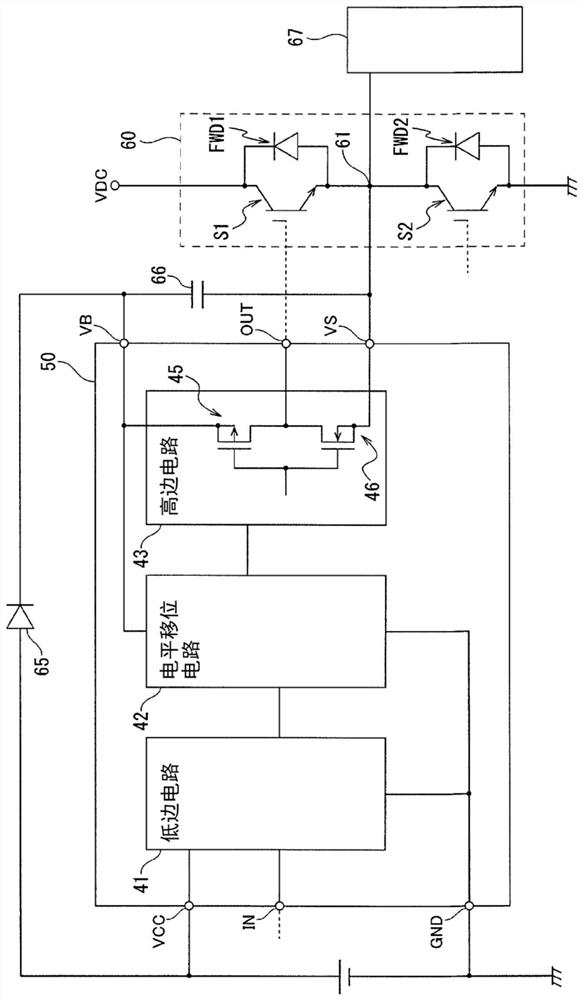
[0049] As the semiconductor device according to the first embodiment of the present invention, a high withstand voltage integrated circuit (hereinafter referred to as “HVIC”) that drives power switching elements constituting a bridge circuit for power conversion or the like is exemplified. Such as figure 1 As shown, the semiconductor device 50 according to the first embodiment of the present invention drives, for example, the power conversion unit 60 that is one phase of a bridge circuit for power conversion. In the power conversion unit 60 , the high-voltage side switching element S1 and the low-voltage side switching element S2 are connected in series to form an output circuit.

[0050]exist figure 1 In the above, the case where the high-voltage side switching element S1 and the low-voltage side switching element S2 are respectively IGBTs is exemplified, but the high-voltage side switching element S1 and the low-voltage side switching element S2 are not limited t...

no. 2 approach

[0098]

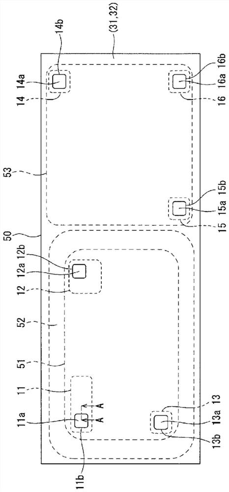
[0099] As the semiconductor device according to the second embodiment of the present invention, an HVIC is exemplified similarly to the semiconductor device according to the first embodiment of the present invention. Such as Figure 12 As shown, the semiconductor device according to the second embodiment of the present invention has wiring layers (high potential side wiring layers) 81 , 82 , and 83 in the uppermost layer of the multilayer wiring structure on the semiconductor substrate. Parts of the high-potential-side wiring layers 81 and 82 constitute pads (high-potential-side pads) 81a and 82a. The high potential side pads 81a, 82a are partitioned by openings 81b, 82b of a surface protection film (not shown). exist Figure 12 In , the openings 81b and 82b of the surface protection film are shown by dashed-dotted lines. The high-potential-side wiring layer 83 constitutes a meandering wiring pattern.

[0100] exist Figure 13 The left and right are shown side ...


PUM

PropertyMeasurementUnit
thicknessaaaaaaaaaa
thicknessaaaaaaaaaa

Abstract

Provided is a semiconductor device capable of preventing, inter alia, the decomposition reaction of an antireflection film provided on a semiconductor substrate and the corrosion of a wiring layer, and capable of improving reliability. The semiconductor device comprises: a wiring layer (11); a titanium nitride layer (21) provided on the wiring layer (11); a titanium oxynitride layer (22) provided on the titanium nitride layer (21); a titanium oxide layer (23) provided on the titanium oxynitride layer (22); and surface protective films (31, 32) provided on the titanium oxide layer (23). The semiconductor device also has an opening (11b) that passes through the titanium nitride layer (21), the titanium oxynitride layer (22), the titanium oxide layer (23), and the surface protective films (31, 32) to expose a part of the wiring layer (11), and the exposed part of the wiring layer (11) constitutes a pad (11a).

Description

technical field [0001] The present invention relates to a semiconductor device and a manufacturing method thereof. Background technique [0002] It is known that in a semiconductor device such as a semiconductor integrated circuit (IC), an antireflection film formed of a titanium nitride (TiN) film or the like is formed on a wiring layer formed of aluminum (Al) or the like provided on a semiconductor substrate, thereby Reflection (halation) of light from a substrate when forming a resist pattern for patterning a wiring layer is reduced (see Patent Documents 1 to 5). [0003] Patent Documents 1 to 4 disclose that a single-layer TiN film is formed on a wiring layer as an antireflection film. Patent Document 5 discloses a laminated structure in which a lower titanium (Ti) film and an upper TiN film are formed on a wiring layer, and the composition ratio of the TiN film is continuously changed. Patent Document 6 discloses that the barrier metal film under the wiring layer is f...

Claims


Application Information

Patent Timeline
Patent Type & Authority Applications(China)
IPC IPC(8): H01L23/532H01L23/522H01L21/768H01L21/60
CPCH01L23/53295H01L23/522H01L21/76832H01L24/13H01L24/11H01L2224/10H01L2224/11H03K2217/0063H03K2217/0081H01L24/05H01L2224/04042H01L23/291H01L2224/0345H01L2224/0391H01L2224/05567H01L24/02H01L2224/0235H01L24/03H01L23/3157H02M1/08H02M7/003H02M7/5387H01L2224/0239H01L2224/05624H01L2924/00014H01L2924/00012H01L2924/0133H01L2924/01014H01L2924/01029H01L2924/0132H01L2924/01013H01L21/76834H01L23/53223H03K17/567
Inventor 山路将晴狩野太一澄田仁志伊藤秀昭
Owner FUJI ELECTRIC CO LTD
Why Eureka
Try Eureka