

Additives for Alkaline Polishing of Single Crystal Silicon Chips and Their Applications
A silicon wafer alkali and additive technology, applied in the direction of single crystal growth, single crystal growth, crystal growth, etc., can solve the problems of poor stability, pyramid residue, low reflectivity, etc., achieve electrical performance gain, improve efficiency, high reflectivity Effect
- Summary
- Abstract
- Description
- Claims
- Application Information
AI Technical Summary
Problems solved by technology
Method used
Image

Examples
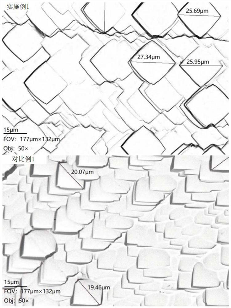
Embodiment 1
[0041] Get 2.5L alkali throw tank, add 2L water, raise temperature to 65 ℃, then add 100mL of 48% NaOH, add 30ml of additive of the present invention after temperature stabilizes (formulation is: 0.05wt% ethyl vanillin , 1wt% polyphosphate, 3wt% disodium tetraacetate, 0.08wt% benzotriazole, and the balance is deionized water); after stirring evenly, remove the silicon wafer with PSG, and place it in NaOH and hydrogen peroxide at 45°C Pre-clean in the tank for 2 minutes. After the pre-cleaning is completed, put it in the water tank for 2 minutes, then put the silicon wafer in the alkali polishing tank for polishing for 4 minutes, and then put it in the water tank for 2 minutes after polishing. The alkali polishing etching process is completed.
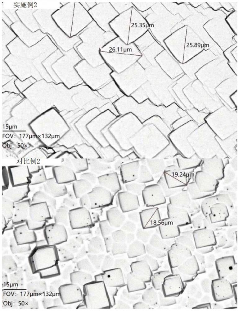
Embodiment 2
[0047] Get 2.5L alkali throw tank, add 2L water, raise temperature to 65 ℃, then add 100mL of 48% NaOH, add 30ml of additive of the present invention after temperature stabilizes (formulation is: 0.05wt% ethyl vanillin , 1wt% polyphosphate, 3wt% disodium tetraacetate, 0.08wt% benzotriazole, and the balance is deionized water) to prepare a polishing liquid; place the polishing liquid for use after three months. Stir the polishing solution evenly, remove the PSG silicon wafer, and perform a pre-cleaning in a tank of NaOH and hydrogen peroxide at 45°C for 2 minutes. After the polishing is completed, put it into the water tank for cleaning for 2 minutes, and the alkali polishing etching process is completed.
Embodiment 3
[0052] Get 150L of alkali throw tank, add 140L of water, temperature is raised to 65 ℃, then add 6L of 48% NaOH, after the temperature stabilizes, add 3.5L of the additive of the present invention (formulation is: 0.05wt% ethyl vanillin , 1wt% polyphosphate, 3wt% disodium tetraacetate, 0.08wt% benzotriazole, and the balance is deionized water); after stirring evenly, 1200 pieces of silicon wafers without PSG were polished. Pre-clean in the tank of NaOH and hydrogen peroxide for 2 minutes. After the pre-cleaning is completed, put it in the water tank for 2 minutes, then put the silicon wafer in the alkali polishing tank for polishing for 4 minutes, and then put it in the water tank for 2 minutes after polishing. The alkali polishing etching process is completed. ; Then enter the follow-up solar cell preparation process to obtain finished solar cell sheets.
PUM
| Property | Measurement | Unit |
|---|---|---|
| reflectance | aaaaa | aaaaa |
Abstract
Description
Claims
Application Information