MEMS humidity sensor based on phase detection principle and preparation method
A technology of humidity sensor and phase detection, which is applied in the process of producing decorative surface effects, the coupling of optical waveguides, and the manufacture of microstructure devices. It can solve the problems of difficult and accurate measurement of humidity, and achieve low price and zero DC power consumption. , Improve the effect of integration
- Summary
- Abstract
- Description
- Claims
- Application Information
AI Technical Summary
Problems solved by technology
Method used
Image
Examples
Embodiment 1
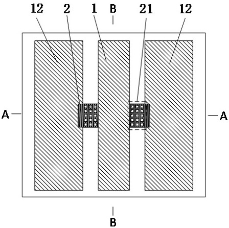
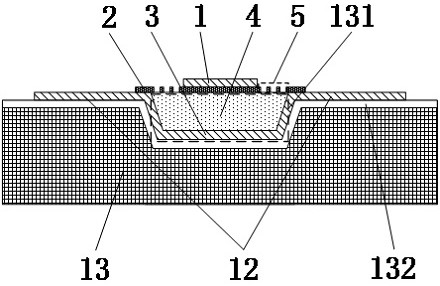
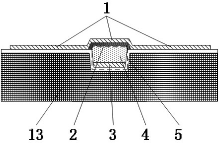
[0029] This embodiment provides a MEMS humidity sensor based on phase detection principle, such as Figure 1 ~ Figure 3 As shown, it includes: a CPW transmission line, a substrate 13 , a groove 131 , a buffer medium layer 132 , a MEMS film 2 , a MEMS beam 3 , a moisture sensing layer 4 and a through hole 5 .
[0030] Specifically, the CPW transmission line is arranged horizontally on the substrate 13, including the CPW signal line 1 located in the middle of the substrate 13 and two CPW ground lines 12 located on both sides of the CPW signal line 1, the CPW signal line 1 and the CPW ground line 12 Can be arranged parallel to each other.
[0031] The groove 131 is located on the substrate 13 directly below the CPW signal line 1, the groove 131 is, for example, a U-shaped groove, and the central axis of the groove 131 is parallel to the CPW signal line 1; the surface of the substrate 13 and the groove 131 is provided with a buffer medium layer 132.
[0032] The MEMS beam 3 is a...
Embodiment 2
[0037] The present invention also provides the preparation method of the above MEMS humidity sensor based on the phase detection principle, such as Figure 4-9 shown, including the following steps:
[0038] S10 prepares a substrate, which may be a common semiconductor substrate, such as a silicon substrate, using high-resistance silicon with a resistivity greater than 1 kΩ·cm. The higher the resistance of the silicon substrate, the CPW is made on silicon, the RF signal loss of its transmission is low, and the RF performance will be better. If the external humidity changes cause capacitance changes, the phase change of the RF signal will be more obvious.
[0039] A groove 131 is etched on the substrate, and then a buffer dielectric layer 132 is grown on the substrate by thermal oxidation, such as Figure 5 As shown, wherein the depth of the groove is, for example, 1-10 μm;
[0040]S20 sequentially passes photolithography, evaporation, and lift-off on the buffer medium layer t...
PUM
| Property | Measurement | Unit |
|---|---|---|
| Depth | aaaaa | aaaaa |
| Thickness | aaaaa | aaaaa |
| Thickness | aaaaa | aaaaa |
Abstract
Description
Claims
Application Information


