Chemically amplified positive ultraviolet photoresist, and preparation method and using method thereof
A technology of ultraviolet light and photoresist, applied in the field of photoresist, can solve the problems of chemically amplified positive ultraviolet photoresist cracking, etc., and achieve the effect of improving brittle crack defects and expanding the scope of application
- Summary
- Abstract
- Description
- Claims
- Application Information
AI Technical Summary
Problems solved by technology
Method used
Image
Examples
preparation example Construction
[0079] The second aspect of the present invention provides a method for preparing the chemically amplified positive UV photoresist, comprising the following steps: quenching the poly(p-hydroxystyrene) polymer resin, the photoacid generator, and the acid After the agent, the crosslinking agent, the leveling agent and the solvent are mixed in proportion, the chemically amplified positive UV photoresist is obtained.
[0080] Preferably, after all the raw materials are mixed, the preparation method includes filtration, for example, a microporous membrane filter can be used for filtration.
[0081] More preferably, the filter pore size is 1-5 μm, such as 1-3 μm or 3-5 μm.
[0082] The third aspect of the present invention provides a method for using the above-mentioned chemically amplified positive UV photoresist, comprising the following steps: coating the chemically amplified positive UV photoresist on a silicon wafer, followed by pre-baking, exposure, and After baking and devel...
Embodiment 1
[0100] A chemically amplified positive UV photoresist comprising the following components in parts by weight (100 parts in total):
[0101]
[0102] The preparation process of the photoresist is as follows: add each component according to the formula, stir to achieve complete dissolution, and complete the preparation of the photoresist after filtering through a polypropylene (PP) microporous filter membrane with a pore size of 1 μm.
[0103] The prepared photoresist is used according to the following method:
[0104] Spin-coat on a 4-inch silicon wafer, then pre-bake at 130°C for 5 minutes, and then expose in an LED 365nm contact exposure machine with an exposure energy of 350mJ / cm 2 , and then post-baked at a temperature of 110° C. for 2 minutes, and then developed, wherein the developing time was 3 minutes, and the developing solution was an aqueous solution of tetramethylammonium hydroxide with a concentration of 2.38%.
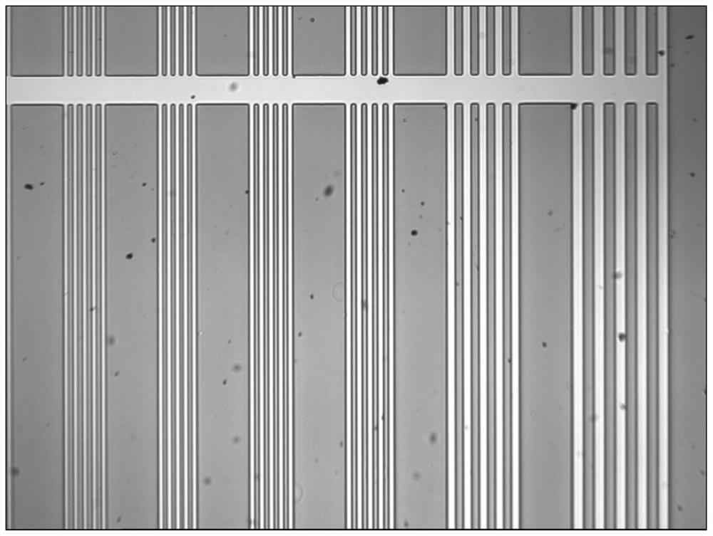
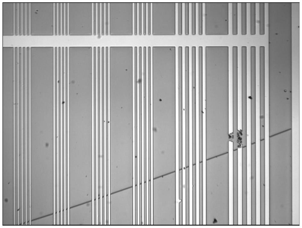
[0105] Obtain a photolithographic pattern such a...
Embodiment 2
[0112] A chemically amplified positive UV photoresist comprising the following components in parts by weight (100 parts in total):
[0113]
[0114] The preparation method of the above-mentioned photoresist is the same as that of Example 1, and the method of using the above-mentioned photoresist is the same as that of Example 1.
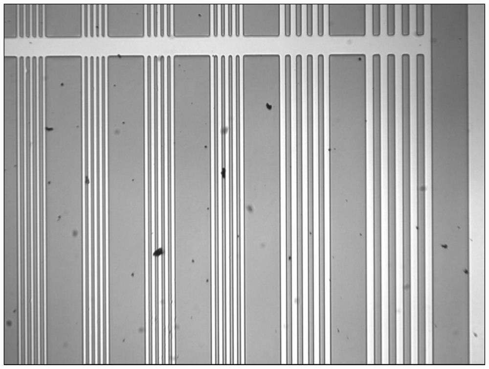
[0115] The obtained lithographic pattern is as image 3 As shown, the film thickness is 20.1 μm, and the cracking of the coating film is observed through the optical microscope OM. The specific results are shown in Table 1.
PUM
| Property | Measurement | Unit |
|---|---|---|
| pore size | aaaaa | aaaaa |
| thickness | aaaaa | aaaaa |
| thickness | aaaaa | aaaaa |
Abstract
Description
Claims
Application Information


