Transistor with local bottom gate and manufacturing method thereof

A manufacturing method and transistor technology, applied in semiconductor/solid-state device manufacturing, semiconductor devices, electrical components, etc., can solve problems such as unfavorable gate control, poor process repeatability, unstable interface, etc., and achieve good thermal stability and strong process compatibility Sexuality, the effect of good interface characteristics

Pending Publication Date: 2021-11-23
BEIJING HUA TAN YUAN XIN ELECTRONICS TECH CO LTD
View PDF4 Cites 0 Cited by
  • Summary
  • Abstract
  • Description
  • Claims
  • Application Information

AI Technical Summary

Problems solved by technology

However, there are still many problems in the low-dimensional material transistors prepared by the above two methods. Taking carbon nanotube transistors as an example, the threshold voltage of high-k dielectric transistors prepared by using metal materials with matching metal work functions to form the source and drain electrodes cannot be effectively adjusted. , the drain terminal is prone to reverse tunneling in the off state, causing problems such as a decrease in the switching ratio
Transistors prepared by using a local bottom gate combined with electrostatic doping on the channel surface, or a top gate structure using electrostatic doping of gate dielectric oxides, currently achieve electrostatic doping usually using incomplete metal oxides (that is, there are more Many oxygen vacancies or dangling bonds, etc.), the interface is unstable, and there are many defect states and interface states, which will reduce the channel mobility, which is not conducive to gate control, affect the uniformity of the device, and the process repeatability is poor.

Method used


Image

  • Transistor with local bottom gate and manufacturing method thereof
  • Transistor with local bottom gate and manufacturing method thereof
  • Transistor with local bottom gate and manufacturing method thereof

Examples


Embodiment Construction

[0071] Embodiments of the present invention will be described in detail below with reference to the accompanying drawings. In the various drawings, the same elements are denoted by the same reference numerals, and various parts in the drawings are not drawn to scale. Also, some well-known parts may not be shown. For the sake of simplicity, the semiconductor structure obtained after several steps can be described in one figure.

[0072] It should be noted that, in the case of no conflict, the embodiments in the present application and the features in the embodiments can be combined with each other. The present invention will be described in detail below with reference to the accompanying drawings and examples.

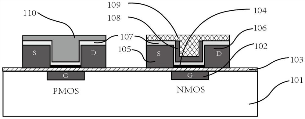
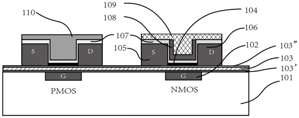
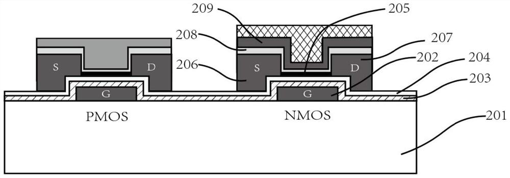
[0073] The structure of the present embodiment with the localized bottom-gate transistor is as follows figure 1 As shown, the transistor includes a substrate 101 in which a local bottom gate 102 is embedded. In this embodiment, the above-mentioned substrate 101 is a...


PUM

PropertyMeasurementUnit
thicknessaaaaaaaaaa

Abstract

The invention relates to a transistor with a local bottom gate and a manufacturing method of the transistor. The transistor comprises a substrate, a low-dimensional semiconductor layer, a source electrode, a drain electrode and the local bottom gate; the local bottom gate is located on the substrate, a gate dielectric layer is arranged on the local bottom gate, the low-dimensional semiconductor layer is located on the gate dielectric layer to serve as a channel of a transistor device, the source electrode and the drain electrode are located on the two opposite sides of the low-dimensional semiconductor channel and make contact with one or more parts of the low-dimensional semiconductor layer respectively; a transition layer and an electrostatic doping layer are arranged on the source electrode, the drain electrode and the channel layer, and fixed charges are arranged in the electrostatic doping layer, so that electrostatic doping is carried out on the corresponding low-dimensional semiconductor channel layer to form an NMOS device, and meanwhile, the invention also provides a manufacturing method of the transistor. The transistor provided by the invention has the advantages of good thermal stability, accurate and controllable threshold voltage and compatibility in process, and can meet the requirements of large-scale carbon-based integrated circuit production.

Description

technical field [0001] The invention relates to the field of semiconductor devices, in particular to a transistor with a partial bottom gate and a preparation method thereof. Background technique [0002] Low-dimensional semiconductor materials, such as carbon nanotubes, graphene, black phosphorus, or two-dimensional materials, are widely used due to their excellent properties such as thin thickness, high mobility, high physical and chemical stability, and high thermal conductivity. Used as a channel material in transistors. Similar to the traditional semiconductor process, transistors with low-dimensional materials as the channel can also change the distribution of carriers in the semiconductor channel material by doping the low-dimensional material, thereby changing its electrical properties and forming p-type regions respectively And n-type regions, and then form semiconductor devices with various structural functions, such as diodes, field effect transistors, etc. Howe...

Claims


Application Information

Patent Timeline
Patent Type & Authority Applications(China)
IPC IPC(8): H01L29/40H01L29/78H01L21/02H01L21/8238
CPCH01L29/408H01L29/78H01L29/66477H01L21/02192H01L21/8238
Inventor 许海涛高宁飞
Owner BEIJING HUA TAN YUAN XIN ELECTRONICS TECH CO LTD
Why Eureka
Try Eureka