Check patentability & draft patents in minutes with Patsnap Eureka AI!

Semiconductor structure preparation method and semiconductor structure

A semiconductor and mask layer technology, applied in semiconductor/solid-state device manufacturing, transistors, electrical components, etc., can solve problems affecting pattern transfer, required pattern deviation, bit line contact structure deviation, etc., to avoid alignment deviation effect of shifting, improving alignment accuracy, and improving performance

Pending Publication Date: 2021-11-30
CHANGXIN MEMORY TECH INC
View PDF7 Cites 0 Cited by
  • Summary
  • Abstract
  • Description
  • Claims
  • Application Information

AI Technical Summary

Problems solved by technology

[0002] In the manufacturing technology of semiconductor structures, the photoresist and mask layer are usually used to form the required pattern in combination with photolithography and etching processes. However, due to the influence of the material properties of the mask layer, the required pattern formed deviates Yield of semiconductor structures
[0003] Taking the manufacture of Dynamic Random Access Memory (DRAM for short) as an example, in the formation process of the bit line contact structure (Bit Line Contact, BLC for short) of DRAM, pattern transfer (transfer) is carried out in dry etching. ) process, because the mask layer is prone to lateral etching, causing the sidewall of the mask layer to form a bowing bend, which affects the transfer of the pattern, which in turn leads to the subsequent formation of bit line contact structures or bit line contact structures A bridge is formed between the active regions, affecting the performance of DRAM
[0004] In addition, with the increase of DRAM integration, the existing technology is more likely to cause the offset of the bit line contact structure, and also cause the formation of connection bridges between the bit line contact structures or between the bit line contact structure and the active region. Affects the performance of DRAM

Method used


Image

  • Semiconductor structure preparation method and semiconductor structure
  • Semiconductor structure preparation method and semiconductor structure
  • Semiconductor structure preparation method and semiconductor structure

Examples


Embodiment Construction

[0029] The method for preparing the semiconductor structure provided by the present invention and the specific implementation of the semiconductor structure will be described in detail below in conjunction with the accompanying drawings.

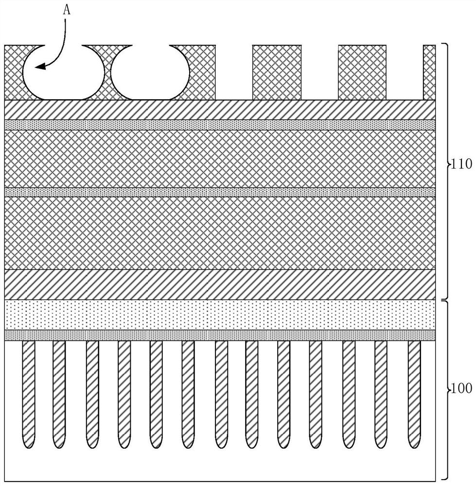
[0030] Figure 1A is a schematic top view of the semiconductor structure provided by the first embodiment of the present invention, please refer to Figure 1A , the semiconductor structure includes a substrate 100 and a mask layer 110 disposed on the substrate 100. When patterning the top mask layer, since the material hardness of the top mask layer is small, the side of the top mask layer The wall will form an arcuate bend (eg Figure 1A The area indicated by the middle arrow A). Then when pattern transfer is performed based on the pattern of the top mask layer, such as Figure 1B and Figure 1C As shown, among them, Figure 1B is a schematic top view of the mask layer 110 of the semiconductor structure, Figure 1C for along Figure ...


PUM

PropertyMeasurementUnit
Angleaaaaaaaaaa

Abstract

The invention provides a semiconductor structure preparation method and the semiconductor structure, which are applied to the field of integrated circuit manufacturing. The preparation method can prevent the side wall of a mask layer from forming an arch bend in a pattern transfer process, thereby preventing a connection bridge from being formed between subsequently formed electric contact structures, and improving the performance of the semiconductor structure. In addition, according to the preparation method, the position of the contact hole is indirectly defined by using the first isolation strip and the second isolation strip, so that the situation that the position of the contact hole is defined by using a boss is avoided, alignment deviation is avoided, and the alignment precision is greatly improved.

Description

technical field [0001] The invention relates to the field of integrated circuit manufacturing, in particular to a method for preparing a semiconductor structure and the semiconductor structure. Background technique [0002] In the manufacturing technology of semiconductor structures, the photoresist and mask layer are usually used to form the required pattern in combination with photolithography and etching processes. However, due to the influence of the material properties of the mask layer, the required pattern formed deviates Yield of semiconductor structures. [0003] Taking the manufacture of Dynamic Random Access Memory (DRAM for short) as an example, in the formation process of the bit line contact structure (Bit Line Contact, BLC for short) of DRAM, pattern transfer (transfer) is carried out in dry etching. ) process, because the mask layer is prone to lateral etching, causing the sidewall of the mask layer to form a bowing bend, which affects the transfer of the pa...

Claims


Application Information

Patent Timeline
IPC IPC(8): H01L21/8242H01L27/108
CPCH10B12/30H10B12/485
Inventor 宛强占康澍夏军李森刘涛徐朋辉
Owner CHANGXIN MEMORY TECH INC
Features
  • R&D
  • Intellectual Property
  • Life Sciences
  • Materials
  • Tech Scout
  • Unparalleled Data Quality
  • Higher Quality Content
  • 60% Fewer Hallucinations
Learn More