Patterned film preparation method without mask plate
A patterned thin film, no mask technology, applied in ion implantation plating, metal material coating process, coating, etc. Problems such as low utilization rate, to achieve the effect of small distance, short coating distance and high utilization rate
- Summary
- Abstract
- Description
- Claims
- Application Information
AI Technical Summary
Problems solved by technology
Method used
Image
Examples
Embodiment 1
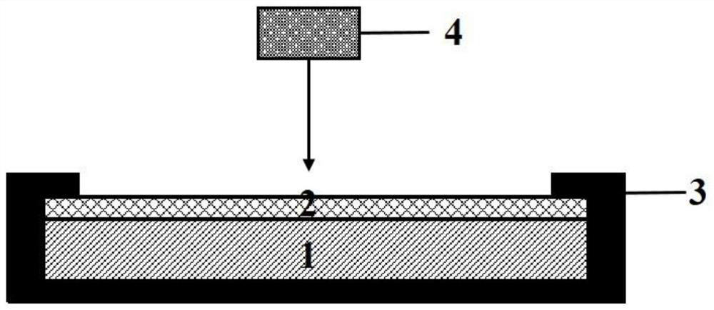
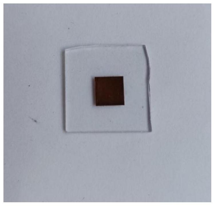
[0051] Such as figure 1 and figure 2 As shown, a method for preparing a patterned film by laser direct writing on a small-sized substrate comprises the following steps:
[0052] 1) Clean the substrate 1 to be plated. The substrate 1 to be plated is a quartz plate. The substrate 1 to be plated is sequentially immersed in acetone, ethanol, and DI water for ultrasonic cleaning for 5 minutes, and then rinsed with DI water. After cleaning, the substrate is dried.
[0053] 2) Fixing the base to be plated 1 and the coating material 2 . The coating material 2 is a copper sheet; the substrate to be plated 1 is placed below, and the coating material 2 is placed on the top and fixed with a clamp 3 .
[0054] 3) Pattern design and parameter setting. Copper sheets are processed by laser scanning set by software installed on a computer. Set a square pattern with a size of 2×2cm on the software, and process it with a laser with a scanning speed of 10mm / s and a power of 1.8W.
[0055] ...
Embodiment 2
[0057] Such as image 3 As shown, a method suitable for preparing a patterned film by laser direct writing on a large-scale substrate differs from Example 1 in that:
[0058] Step 1) Cleaning the substrate 1 to be plated. The substrate 1 to be plated is glass. The substrate 1 to be plated is directly rinsed with a DI water gun. After cleaning, the substrate 1 to be plated is blown dry with a nitrogen gun.
[0059] Step 2) The substrate to be plated 1 and the coating material 2 are fixed. The coating material 2 is copper foil; the base 1 to be plated is placed below, and the surroundings of the coating material 2 are bonded to the base 1 to be plated.
[0060] Step 4) Using the laser light source 4 to scan and irradiate the fixed substrate 1 to be coated and the coating material 2 . The diameter of the laser spot is set to 10 microns, the laser scanning distance is 1 mm, the laser bombards the coating material 2, and the copper clusters produced by the bombardment are sputter...
Embodiment 3
[0062] Such as Figure 4 As shown, the difference between this embodiment and embodiment 1 is:
[0063] Step 4) Laser direct writing. Set the laser program to triangle, pentagon and English letter "UJN", write the coating material 2 copper foil directly onto the substrate to be plated 1 quartz, such as Figure 4 SEM patterns of different patterns.
PUM
 Abstract
Description
Claims
Application Information
 - R&D
- Intellectual Property
- Life Sciences
- Materials
- Tech Scout
- Unparalleled Data Quality
- Higher Quality Content
- 60% Fewer Hallucinations
Browse by: Latest US Patents, China's latest patents, Technical Efficacy Thesaurus, Application Domain, Technology Topic, Popular Technical Reports.
© 2025 PatSnap. All rights reserved.Legal|Privacy policy|Modern Slavery Act Transparency Statement|Sitemap|About US| Contact US: help@patsnap.com


