Integrated circuit optical proximity correction parallel processing method and system

A technology of optical proximity correction and parallel processing, which is applied in the direction of originals, optics, and optomechanical equipment for optomechanical processing. It can solve the problem of large correction errors at the boundaries of overlapping regions, reduced correction speed, and data that do not meet the mask requirements. Problems such as manufacturing rules can save computing resources and time, improve speed, and avoid correction of boundary problems

Inactive Publication Date: 2021-12-10
珠海市睿晶聚源科技有限公司
View PDF4 Cites 0 Cited by
  • Summary
  • Abstract
  • Description
  • Claims
  • Application Information

AI Technical Summary

Problems solved by technology

The overlapping parts cause repeated calculations, further reducing the speed of the overall correction
In addition, some graphics inevitably span multiple blocks. After these graphics are divided into different blocks, the edge offset positions of the corrected graphics are different. After merging, the correction error at the boundary of the overlapping area will be large, or the corrected data will not be correct. Issues such as meeting mask manufacturing rules

Method used


Image

  • Integrated circuit optical proximity correction parallel processing method and system
  • Integrated circuit optical proximity correction parallel processing method and system
  • Integrated circuit optical proximity correction parallel processing method and system

Examples


Embodiment

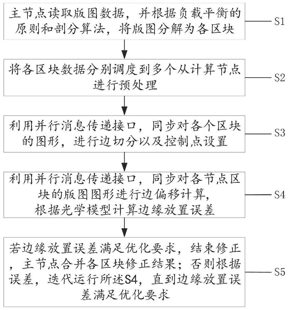
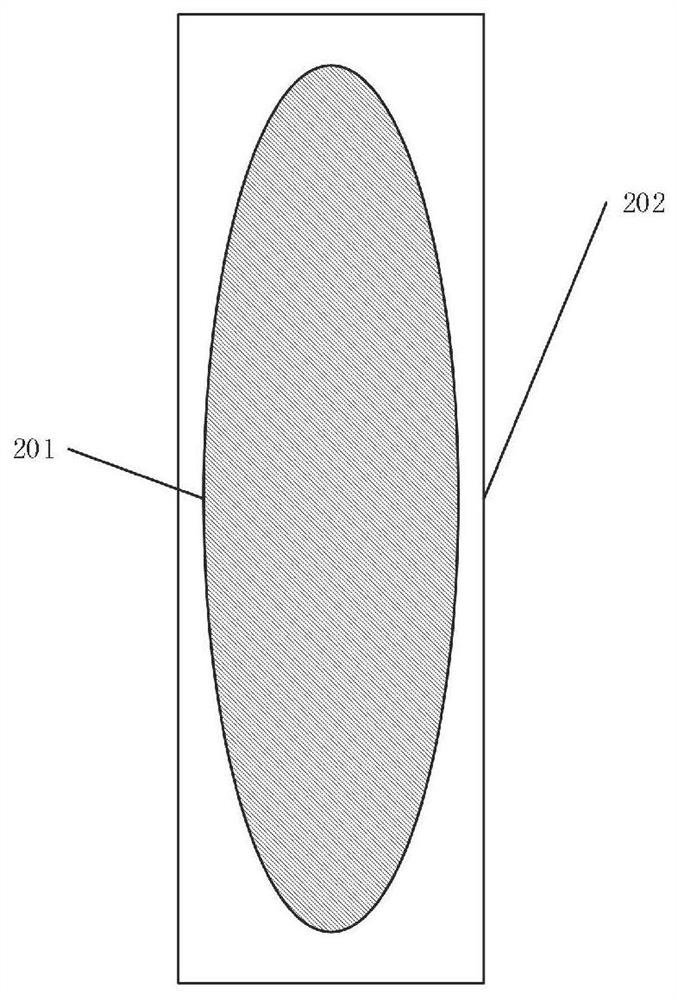
[0036] It should be noted that in semiconductor manufacturing, an important step in the chip process is the use of photolithography. The pattern "negative" used in these steps is called a mask. An opaque graphic mask is masked, so underlying erosion or diffusion will only affect areas outside the selected area. In the field of integrated circuits, feature size refers to the smallest dimension in a semiconductor device. The smaller the feature size, the higher the integration level of the chip. However, in practice, the wavelength of the light source of the existing lithography system is usually much larger than the feature size of the integrated circuit, that is, the resolution of the lithography system is not enough, resulting in serious distortion of the manufactured graphics due to light interference and diffraction effects, and finally processed on the silicon wafer. Lithographic patterns are different from design patterns. Compared with the original layout, the imaging ...


PUM


Abstract

The invention discloses an integrated circuit optical proximity correction parallel processing method and system. The method is characterized in that the method comprises the following steps: S1, reading layout data through a main node, and decomposing a layout into blocks according to a load balance principle and a subdivision algorithm; S2, scheduling the data of each block to a plurality of slave nodes, and preprocessing; S3, synchronously carrying out edge segmentation and control point setting on the graph of each block by utilizing a parallel message passing interface; S4, synchronously carrying out edge offset calculation on the layout graph of each node block by utilizing a parallel message passing interface, and calculating an edge placement error according to an optical model; and S5, if the edge placement error meets the optimization requirement, finishing the correction, and combining the correction results of the blocks by the main node; if not, iteratively operating step S4 according to the error until the edge placement error meets the optimization requirement. According to the method, the edge offset information of each iterative calculation of the overall layout data can be synchronized, and the calculated correction graph splicing is ensured to be abnormal through rule constraint.

Description

technical field [0001] The invention relates to the technical fields of computer-aided design and semiconductor manufacturing, in particular to a method and system for parallel processing of integrated circuit optical proximity correction. Background technique [0002] Photolithography is the core step in the manufacture of integrated circuits. Photolithography realizes the transfer of the design layout to the surface pattern of the silicon wafer. The quality of lithography and the resolution determine the key process of the size that the integrated circuit can achieve. With the continuous reduction of the feature size of the integrated circuit process, the design size is close to the limit of the theoretical resolution of the lithography exposure system. When the feature size of the integrated circuit is smaller than the wavelength of the light source of the photolithography system, the manufacturing pattern will be seriously distorted due to the interference and diffracti...

Claims


Application Information

Patent Timeline
Patent Type & Authority Applications(China)
IPC IPC(8): G03F1/36G03F7/20
CPCG03F1/36G03F7/70441
Inventor 赵西金胡滨
Owner 珠海市睿晶聚源科技有限公司
Why Eureka
Try Eureka