

Bulk heterojunction organic field effect transistor memory and preparation method thereof
A technology of bulk heterojunction and organic field, which is applied in the manufacture of semiconductor/solid-state devices, electric solid-state devices, semiconductor devices, etc., can solve the problems of unstable operation and complex preparation process of heterojunction field-effect transistor memory, and achieve the goal of manufacturing The method is simple and easy, the effect of improving mobility and threshold voltage, and high repetition rate
- Summary
- Abstract
- Description
- Claims
- Application Information
AI Technical Summary
Problems solved by technology
Method used
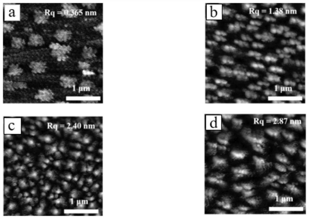
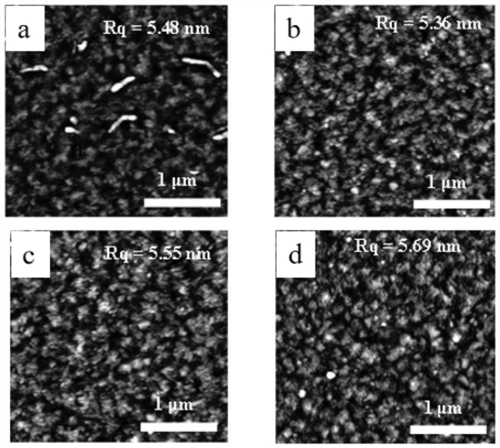
Image

Examples
preparation example Construction
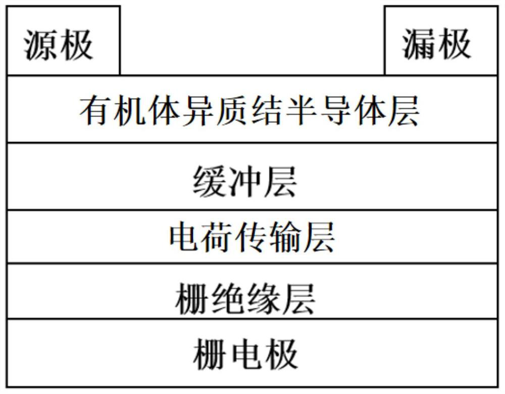
[0042] The present invention also provides a method for preparing the organic field-effect transistor memory with bipolar memory performance produced by the organic heterojunction semiconductor layer, which specifically includes the following steps:
[0043] (1) Configure the charge transport layer solution: dissolve the polymer tetramethylpiperidinol TMP in the organic solvent toluene to form a polymer solution, heat in a water bath for 2h to completely dissolve the polymer tetramethylpiperidinol TMP, and the TMP in the solution The concentration is 3mg / ml;
[0044] (2) Prepare the substrate: select n-type heavily doped silicon as the substrate, including the lower gate electrode and the upper thermally grown 50nm silicon dioxide as the gate insulating layer, and cut the substrate into 1.5×1.5cm 2 According to the specifications, place it on a shelf at an angle of 45°, put it in a beaker, add acetone to immerse the silicon wafer substrate, ultrasonicate for 15 minutes, and po...
Embodiment 1
[0053] (1) Prepare tetramethylpiperidinol TMP solution with a concentration of 3 mg / ml, which needs to be prepared at least 2 hours in advance to ensure that tetramethylpiperidinol is fully dissolved, and the solvent is toluene without additional treatment;
[0054] (2) Prepare the substrate: select n-type heavily doped silicon as the substrate, and its surface has SiO with a thermal growth thickness of 50nm 2 Insulation layer, cut the silicon wafer substrate into 1.5×1.5cm 2 placed on a shelf at an angle of 45°, put it in a beaker, add acetone to immerse the silicon wafer substrate, sonicate for 15 minutes, and pour off the acetone; then add ethanol and deionized water, and pour off the ethanol and deionized water after 15 minutes of supersonication , and then dry the surface with nitrogen, and place it in an oven at 120°C for 30 minutes to dry the substrate thoroughly, and then place the dried silicon wafer substrate in a UV cleaning machine for 10 minutes to further clean t...
Embodiment 2
[0061] (1) Prepare tetramethylpiperidinol TMP solution with a concentration of 3 mg / ml, which needs to be prepared at least 2 hours in advance to ensure that tetramethylpiperidinol is fully dissolved, and the solvent is toluene without additional treatment;
[0062] (2) Prepare the substrate: select n-type heavily doped silicon as the substrate, and its surface has SiO with a thermal growth thickness of 50nm 2 Insulation layer, cut the silicon wafer substrate into 1.5×1.5cm 2 placed on a shelf at an angle of 45°, put it in a beaker, add acetone to immerse the silicon wafer substrate, sonicate for 15 minutes, and pour off the acetone; then add ethanol and deionized water, and pour off the ethanol and deionized water after 15 minutes of supersonication , and then dry the surface with nitrogen, and place it in an oven at 120°C for 30 minutes to dry the substrate thoroughly, and then place the dried silicon wafer substrate in a UV cleaning machine for 10 minutes to further clean t...
PUM
| Property | Measurement | Unit |
|---|---|---|
| thickness | aaaaa | aaaaa |
| thickness | aaaaa | aaaaa |
| thickness | aaaaa | aaaaa |
Abstract
Description
Claims
Application Information