Manufacturing method of heterojunction cell , heterojunction cell and solar cell module

A technology of a heterojunction cell and a manufacturing method, applied in the field of solar cells, can solve the problems of poor conductivity of conductive films and high production costs, and achieve the effects of increasing absorption probability, improving internal reflection, and reducing consumption

Pending Publication Date: 2021-12-10
ZHEJIANG AIKO SOLAR ENERGY TECH CO LTD +3
View PDF0 Cites 0 Cited by
  • Summary
  • Abstract
  • Description
  • Claims
  • Application Information

AI Technical Summary

Problems solved by technology

[0004] The invention provides a method for manufacturing a heterojunction battery, aiming to solve the technical problems of poor conductivity and high production cost of the conductive film of the heterojunction battery produced by the existing manufacturing method

Method used


Image

  • Manufacturing method of heterojunction cell , heterojunction cell and solar cell module
  • Manufacturing method of heterojunction cell , heterojunction cell and solar cell module
  • Manufacturing method of heterojunction cell , heterojunction cell and solar cell module

Examples


Embodiment 1

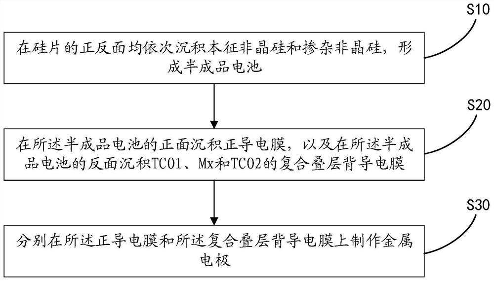
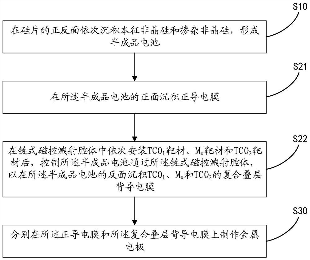
[0044] refer to figure 1 , the first embodiment provides a method for manufacturing a heterojunction battery, including the following steps:

[0045] S10, sequentially deposit intrinsic amorphous silicon and doped amorphous silicon on the front and back of the silicon wafer to form a semi-finished battery;

[0046] S20, depositing a positive conductive film on the front side of the semi-finished battery, and depositing TCO on the back side of the semi-finished battery 1 , M x and TCO 2 Composite laminated back conductive film;

[0047] S30, making metal electrodes on the positive conductive film and the composite laminated back conductive film respectively;

[0048] Among them, TCO 1 and TCO 2 Aluminum-doped zinc oxide, tin-doped indium oxide, indium-doped zinc oxide, gallium-doped zinc oxide, indium-gallium-doped zinc oxide, tungsten-doped indium oxide, molybdenum-doped indium oxide or zirconium-doped indium oxide, M x It is silver, aluminum, copper or silver-copper al...

Embodiment 2

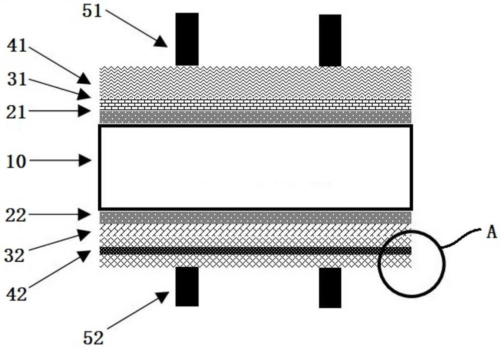
[0070] refer to image 3 , this embodiment 2 provides a heterojunction battery, which is prepared by the manufacturing method of the heterojunction battery as described in the first embodiment, and the heterojunction battery includes:

[0071] Wafer 10;

[0072] Intrinsic amorphous silicon and doped amorphous silicon respectively arranged on the front and back of the silicon wafer 10;

[0073] A positive conductive film 41 disposed on the doped amorphous silicon on the front side, and a TCO disposed on the doped amorphous silicon on the back side 1 , M x and TCO 2 Composite laminate back conductive film 42;

[0074] Metal electrodes respectively arranged on the positive conductive film 41 and the composite laminate back conductive film 42;

[0075] Among them, TCO 1 and TCO 2 is aluminum-doped zinc oxide, tin-doped indium oxide, indium-doped zinc oxide, gallium-doped zinc oxide, indium-gallium-doped zinc oxide, tungsten-doped indium oxide, molybdenum-doped indium oxide ...

Embodiment 3

[0079] The third embodiment provides a solar cell module, including the heterojunction cell as described in the second embodiment. Since the optical properties of the back conductive film of the heterojunction battery are not as high as those of the front conductive film, an ultra-thin metal layer is introduced into the composite laminated back conductive film 42 to greatly improve the conductivity of the back film. The plasmonic enhancement effect improves the internal reflection of long-wavelength transmitted light, increases its absorption probability in the silicon wafer 10, and generates more photocurrent; in addition, because the insertion of an ultra-thin metal layer can greatly improve the conductivity of the back film, It can make the pattern on the back only keep the welding main grid, and no fine grid lines are needed, thereby greatly reducing the consumption of silver paste on the back and reducing the production cost.


PUM

PropertyMeasurementUnit
thicknessaaaaaaaaaa
thicknessaaaaaaaaaa
thicknessaaaaaaaaaa

Abstract

The invention belongs to the technical field of solar cells, and particularly relates to a manufacturing method of a heterojunction cell, the heterojunction cell and a solar cell module. The manufacturing method comprises the following steps: sequentially depositing intrinsic amorphous silicon and doped amorphous silicon on the front and back surfaces of a silicon wafer to form a semi-finished product cell; depositing a front conductive film on the front surface of the semi-finished battery, and depositing a composite laminated back conductive film of TCO1, Mx and TCO2 on the back surface of the semi-finished battery; and respectively manufacturing metal electrodes on the positive conductive film and the composite laminated back conductive film. The ultrathin metal layer is introduced into the composite laminated back conductive film, the conductive performance of the back film is greatly improved, meanwhile, due to the plasma enhancement effect, the internal reflection of long-wavelength transmission light is improved, the absorption probability of the long-wavelength transmission light in a silicon wafer is increased, and more light current is generated; and in addition, due to insertion of the ultrathin metal layer, the conductivity of the back film can be greatly improved, and only a welding main grid is reserved in a back pattern, so that the consumption of back silver paste is greatly reduced, and the production cost is reduced.

Description

technical field [0001] The invention belongs to the technical field of solar cells, and in particular relates to a manufacturing method of a heterojunction cell, a heterojunction cell and a solar cell module. Background technique [0002] At present, heterojunction cells usually use fully transparent conductive film (TCO) indium tin oxide (ITO) as the conductive channel on the back. The main preparation method is magnetron sputtering. First, the intrinsic amorphous is sequentially deposited on the front and back of the silicon wafer. Silicon and doped amorphous silicon, and then deposit ITO layers on the front and back of the semi-finished battery under low temperature conditions, and finally print silver paste to build the front and back electrodes, and sinter at a temperature below 250°C to achieve ohmic contact. [0003] However, the conductivity of the ITO thin film deposited at low temperature is poor, resulting in low photoelectric conversion efficiency of the final he...

Claims


Application Information

Patent Timeline
Patent Type & Authority Applications(China)
IPC IPC(8): H01L31/20H01L31/02H01L31/054H01L31/0747
CPCH01L31/202H01L31/0747H01L31/02008H01L31/0547Y02E10/52Y02P70/50
Inventor 张生利王永谦林纲正陈刚
Owner ZHEJIANG AIKO SOLAR ENERGY TECH CO LTD
Why Eureka
Try Eureka