Method for growing large-scale IV-VI group compound single crystal thin film material by PVD technology

A IV-VI, single crystal thin film technology, applied in chemical instruments and methods, single crystal growth, single crystal growth, etc., can solve the problems of experimental exploration limitations, constrained applications, unrealized large-scale GeSe single crystal thin films, etc. , to achieve the effect of low experimental cost, less consumables and strong binding force

Active Publication Date: 2021-12-14
CHONGQING INST OF GREEN & INTELLIGENT TECH CHINESE ACADEMY OF SCI +1
View PDF5 Cites 1 Cited by
  • Summary
  • Abstract
  • Description
  • Claims
  • Application Information

AI Technical Summary

Problems solved by technology

However, the experimental preparation of large-scale GeSe single crystal thin films has not yet been realized, so the experimental exploration of the material's anisotropic c...

Method used


Image

  • Method for growing large-scale IV-VI group compound single crystal thin film material by PVD technology
  • Method for growing large-scale IV-VI group compound single crystal thin film material by PVD technology
  • Method for growing large-scale IV-VI group compound single crystal thin film material by PVD technology

Examples


Embodiment 1

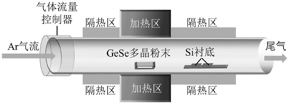
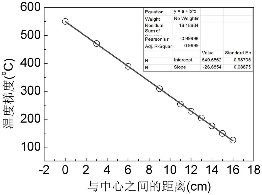
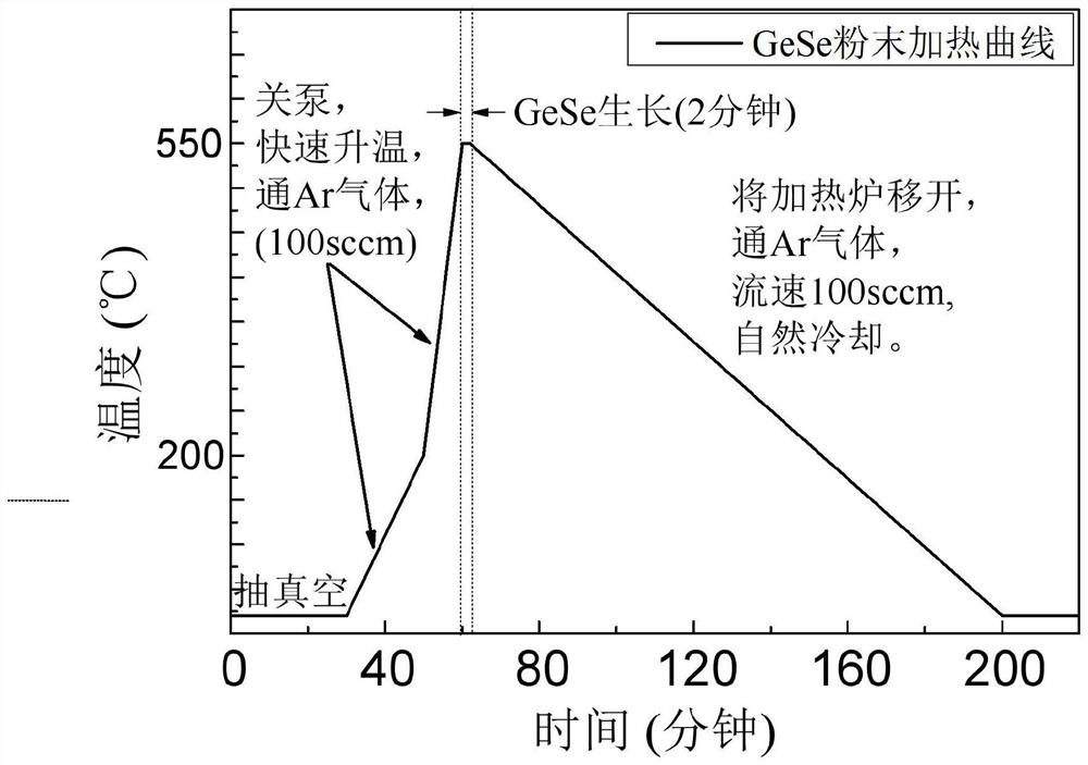
[0037] Embodiment 1 of the present invention provides a method for growing a large-scale GeSe single crystal thin film material by PVD technology, the preparation is carried out in a single heating tube furnace, and the specific structure is as follows figure 1 As shown; with the increase of the length from the heating center, the temperature gradient changes at each position are as follows figure 2 Shown; The schematic diagram of the temperature and airflow settings during the preparation and growth process is shown in image 3 shown.

[0038] Specifically include the following steps:

[0039] (1) The substrate used to prepare the sample is a surface-polished single-crystal silicon wafer or a surface-polished and oxidized single-crystal silicon wafer; before preparing the sample, the substrate needs to be cleaned to remove surface impurities; the substrate is placed in acetone, alcohol, Ultrasonic cleaning in deionized water for 10 minutes; then dry the cleaned substrate w...

Embodiment 2

[0045] The technical solution disclosed in Embodiment 2 of the present invention is basically the same as Embodiment 1, only the high-purity GeSe (99.999%) polycrystalline powder is replaced by high-purity SnS (99.999%) polycrystalline powder.

Embodiment 3

[0047] The technical solution disclosed in Embodiment 3 of the present invention is basically the same as Embodiment 1, except that the high-purity GeSe (99.999%) polycrystalline powder is replaced by high-purity SnSe (99.999%) polycrystalline powder.


PUM


Abstract

The invention discloses a method for growing a large-scale IV-VI group compound single crystal thin film material by a PVD technology. The method specifically comprises three main stages: 1, preparing a material, and optimally selecting the weight of a polycrystalline powder source; 2, placing the powder source and a substrate in a quartz tube, and setting the positions of the powder source and the substrate in the quartz tube; and 3, growing a single crystal film by utilizing the physical vapor deposition technology. A large-scale layered film material with a regular strip shape is prepared by optimizing the heating rate, the heat preservation temperature and time, the substrate temperature and the airflow velocity of a powder source, so that an important technical foundation is laid for experimental preparation and application of a large-scale IV-VI family single crystal film.

Description

technical field [0001] The invention relates to the technical field of new materials, and more specifically relates to a method for growing large-scale IV-VI compound single crystal thin film materials by PVD technology. Background technique [0002] Graphene is made of carbon atoms through SP 2 The three carbon atoms close to it are hybridized to form a 120° σ bond, forming a honeycomb structure. The simple structure of graphene has many unique physical phenomena, including Dirac fermions, fractional and room temperature quantum Hall effect, minimum quantum conduction, etc. Graphene has many good properties, such as the lightest carrier mass, the highest current density, the longest mean free path at room temperature, the highest carrier mobility, etc., among which the ultra-high carrier mobility is Offers potential for developing fast electronic devices. However, the ultrahigh mobility of graphene is caused by zero bandgap, and the lack of an intrinsic bandgap leads to ...

Claims


Application Information

Patent Timeline
IPC IPC(8): C30B29/48C30B23/06C30B23/02
CPCC30B29/48C30B23/063C30B23/002Y02P70/50
Inventor 王春香赵洪泉石轩张国欣张炜
Owner CHONGQING INST OF GREEN & INTELLIGENT TECH CHINESE ACADEMY OF SCI
Why Eureka
Try Eureka