

Method for cleaning indium phosphide substrate wafer
An indium phosphide and wafer technology, which is applied in the application field of semiconductor material production, can solve the problems of excessive surface impurity content, the quality of the wafer needs to be improved, and the high content of sulfur on the surface of the substrate, so as to improve the yield, improve the surface quality of the substrate, Effects of optimization and substrate surface quality
- Summary
- Abstract
- Description
- Claims
- Application Information
AI Technical Summary
Problems solved by technology
Method used
Image

Examples
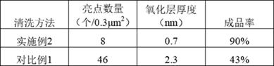
Embodiment 1
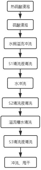
[0034] A kind of cleaning method of indium phosphide substrate wafer, its concrete process flow chart is as figure 1 shown, including:
[0035] (1) Select a group of 20 pieces of indium phosphide 2-inch wafers that have been polished and waxed by waxing and polishing process, and use a special cleaning fixture to take a piece of indium phosphide wafer in order to clamp them. Soak in hot sulfuric acid at ℃ for 5s;
[0036] (2) Soak in sulfuric acid with a mass fraction of 96% at room temperature for 2 seconds, then put it into a water bowl, and use a water gun to rinse the water bowl at the same time to keep the water overflowing. The overflow water volume is 10-50L / min. The bowling time is 5-10s, and the water gun flushing time is 30s;
[0037] (3) Soak in S1 cleaning solution (a mixture of water, hydrogen peroxide and ammonia peroxide with a volume ratio of 1:2:10) at 4°C for 60 seconds, and rotate the wafer clamp continuously during the soaking process to make the surface ...
Embodiment 2
[0044] A kind of cleaning method of indium phosphide substrate wafer, its specific process flow chart is as figure 1 shown, including:
[0045] (1) Select a group of 9 pieces of indium phosphide 3-inch wafers that have been polished and waxed by waxing and polishing process, and use a special cleaning fixture to take a piece of indium phosphide wafer in order to clamp. Soak in hot sulfuric acid at 65°C for 5s;
[0046](2) Soak in sulfuric acid with a mass fraction of 96% and room temperature for 3 seconds; then put it into a water bowl, and at the same time use a water gun to rinse the water bowl to keep the water overflowing. The overflow water volume is 10-50L / min. The time is 5-10s, and the subsequent flushing time is 40s;
[0047] (3) Soak in S1 cleaning solution (a mixture of water, hydrogen peroxide and ammonia peroxide with a volume ratio of 1:2:3) at 4°C for 60s, and rotate the wafer clamp continuously during the soaking process to make the surface of the wafer recei...
PUM
 Abstract
Description
Claims
Application Information