

Method for measuring ferroelectric hysteresis loop between any two points of ferroelectric material without plating electrode
A technology of ferroelectric materials and hysteresis loops, which is applied in the field of hysteresis loops, can solve the problems of cumbersome preparation process, sample surface contamination, inability to measure hysteresis loops of ferroelectric thin films, etc., and achieve the effect of simplifying the measurement process
- Summary
- Abstract
- Description
- Claims
- Application Information
AI Technical Summary
Problems solved by technology
Method used
Image

Examples
Embodiment 1
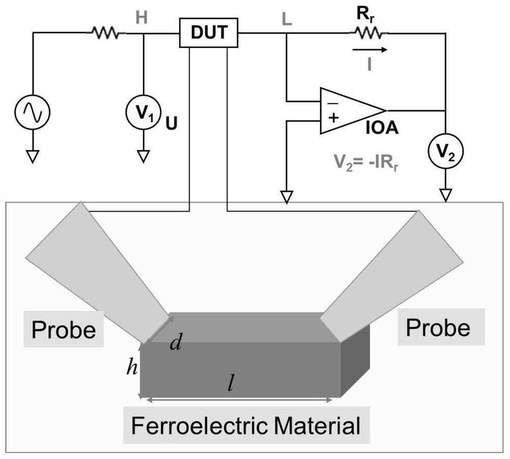
[0041] Step 1. Fix an epitaxial bismuth ferrite thin film with a size of 0.5 mm×0.5 mm grown on a strontium titanate substrate on a probe station, and press two probes on the thin film.
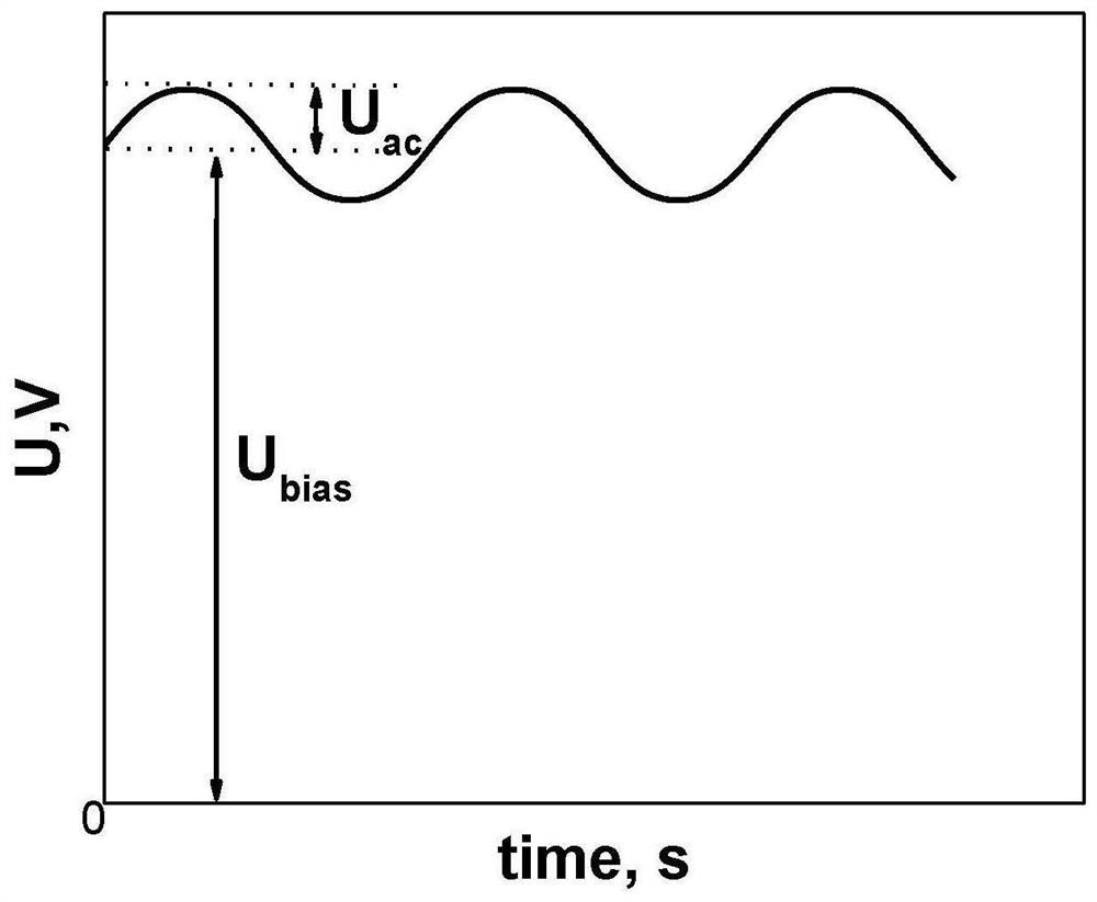
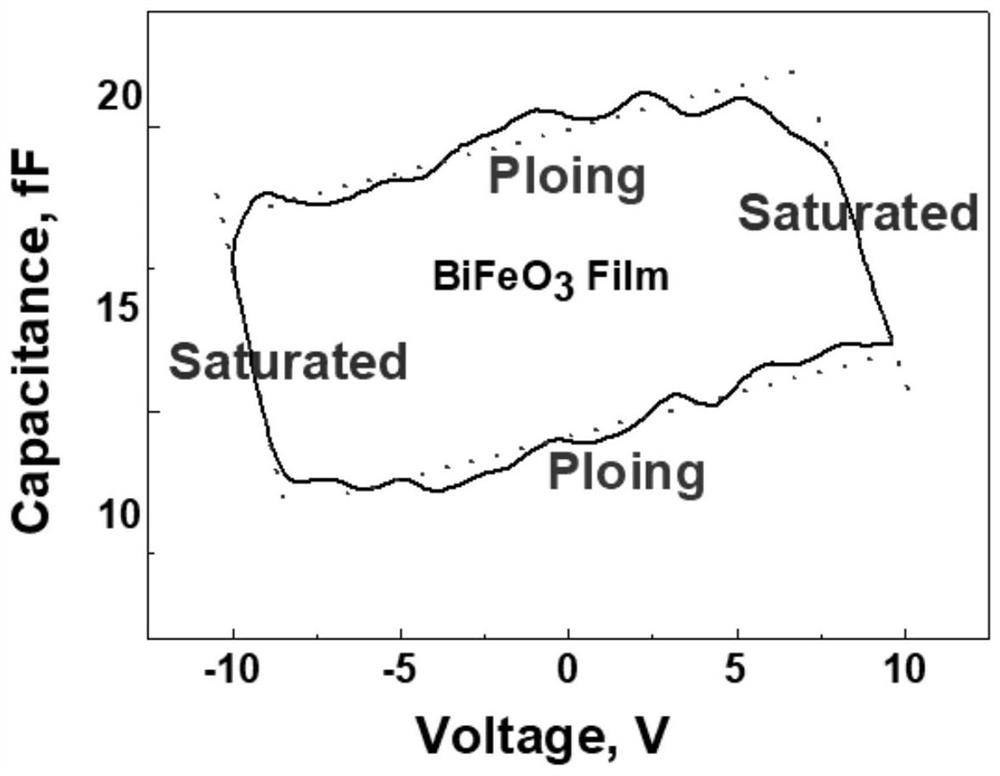
[0042]Step 2. Apply a scanning bias voltage from 10V to -10V and then to -10V through the semiconductor parameter analyzer, and then add an AC voltage signal with an amplitude of 25mV and a frequency of 1MHz to the bias voltage to scan the CV curve. The curve is as follows image 3 shown.
[0043] Step 3, draw the obtained CV curve, perform mathematical processing on the curve, eliminate the influence of leakage conduction, and obtain C act ~ V curve, and then take the average value to get the static capacitance C s , subtract the static capacitance from the measured capacitance to obtain the ferroelectric polarization capacitance C f ~ V curve, such as Figure 4 shown.
Embodiment 2
[0045] Step 1. Fix an epitaxial bismuth ferrite thin film with a size of 0.5 mm×0.5 mm grown on a strontium titanate substrate on a probe station, and press two probes on the thin film.
[0046] Step 2. Apply a 10V to -10V and then to -10V scanning bias through the semiconductor parameter analyzer, respectively add 405nm LED purple light in the dark, and then add a 25mV amplitude and a frequency of 1MHz to the bias voltage. AC voltage signal for CV curve scanning.
[0047] Step 3. Draw the obtained CV curve and perform mathematical processing on the curve to obtain C under dark and light conditions. act ~ V curve such as Figure 5 As shown in (a), then get the ferroelectric polarization capacitance C f ~V curve, the ferroelectric polarization capacitance is multiplied by the amplitude of the applied AC bias voltage of 25mV, then divided by the probe diameter of 0.52mm and film thickness of 10 microns to obtain the ferroelectric polarization intensity, and then the polarizati...
Embodiment 3
[0049] Step 1. Fix the PVDF ferroelectric fiber prepared by electrospinning on the PET substrate on a probe station, and add probes to both ends of a fiber on a microscope.
[0050] Step 2. Apply a 20V to -20V and then to -20V scanning bias through the semiconductor parameter analyzer, and at the same time apply bending deformation to the PET substrate to generate bending strain on the PVDF fiber, and then add an amplitude of 25mV to the bias , the AC voltage signal with a frequency of 1kHz is used to scan the CV curve.
[0051] Step 3. Draw the obtained CV curve, perform mathematical processing on the curve, and measure the leakage conductance under light, linear polarization capacitance, ferroelectric polarization charge, coercive voltage; and Q-V hysteresis loop and P-E hysteresis loop .
PUM
 Abstract
Description
Claims
Application Information