
A layered micro-nano composite structure for enhancing boiling heat transfer and its processing method
A composite structure, enhanced boiling technology, applied in indirect heat exchangers, lighting and heating equipment, cooling/ventilation/heating renovation, etc. Difficult heat transfer enhancement effect, etc., to delay the deterioration of heat transfer, increase the critical heat flux density, and increase the actual heat exchange area.
- Summary
- Abstract
- Description
- Claims
- Application Information
AI Technical Summary
Problems solved by technology
Method used
Image

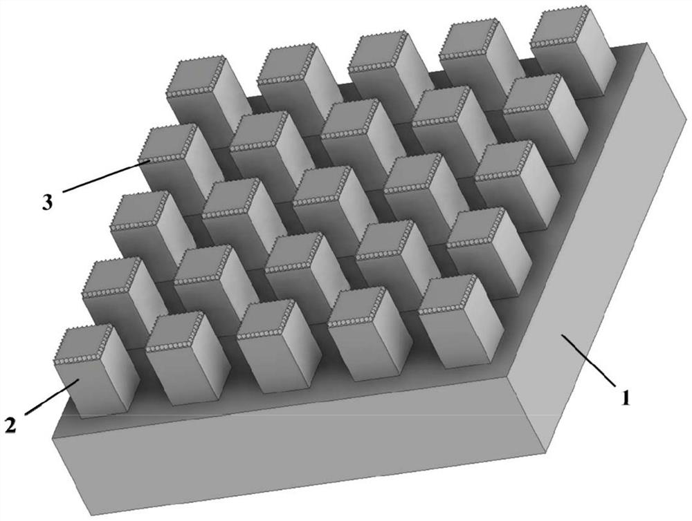
Examples
Embodiment 1
[0035] Objective: To etch a regular array of square pillar microstructures with a pillar width of 20 μm, a pillar height of 120 μm, and a distance between the centers of the micropillars of 60 μm.
[0036] Step 1: Design a corresponding mask pattern according to the etching target, and process the mask.
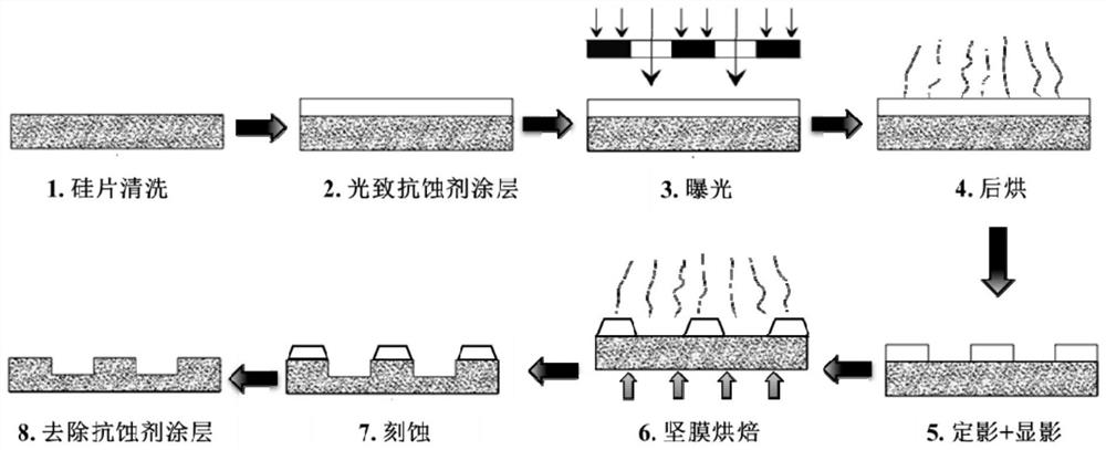
[0037] Step 2: Pre-treat the silicon wafer with HMDS for 10min; then stick it on the glue spinner, rotate forward for 6s at a speed of 600r / min, and reverse for 30s at a speed of 4000r / min, so that the photoresist AZ6130 It is uniformly coated on the front side of the silicon wafer with a coating thickness of 7.5 μm; then the silicon wafer is placed on a contact hot plate at 100°C for 5 minutes before drying to obtain a relatively firm photoresist layer. Then, the silicon wafer was exposed on an MA6 lithography machine for 23s, and placed in a 2.38% TMAH developer solution for 150s to complete the development process. After the inspection is correct, carry out the hard film ...
Embodiment 2
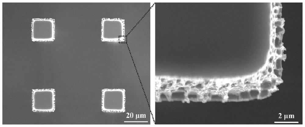
[0039] Goal: To etch a regular array of square-pillar microstructures with a column width of 50 μm, a column height of 60 μm, and a distance between the centers of the micro-pillars of 100 μm, while etching nano-scale holes on the four edges of the top surface of the square column.
[0040] Step 1: Design a corresponding mask pattern according to the etching target, and process the mask.
[0041]Step 2: Pre-treat the silicon wafer with HMDS for 10min; then stick it on the glue dispenser, rotate it forward for 6s at a speed of 600r / min, and reverse it for 30s at a speed of 1000r / min, so that the photoresist AZ6130 It is uniformly coated on the front side of the silicon wafer, and the thickness of the coating is 5.2 μm; then the silicon wafer is placed on a contact hot plate at 100 ° C and dried for 5 minutes to obtain a relatively strong photoresist layer. Then the silicon wafer was exposed on the MA6 lithography machine for 4.2s, and placed in 3038 developer solution for 70s t...
Embodiment 3
[0044] Objective: To etch a regular array of square pillar microstructures with a pillar width of 100 μm, a pillar height of 60 μm, and a center distance of 200 μm between the micropillars, while etching nano-scale holes on the four edges of the top surface of the square pillars.
[0045] Step 1: Design a corresponding mask pattern according to the etching target, and process the mask.
[0046] Step 2: Pre-treat the silicon wafer with HMDS for 10min; then stick it on the glue dispenser, rotate it forward for 6s at a speed of 600r / min, and reverse it for 30s at a speed of 1000r / min, so that the photoresist AZ6130 It is uniformly coated on the front side of the silicon wafer, and the thickness of the coating is 5.2 μm; then the silicon wafer is placed on a contact hot plate at 100 ° C and dried for 5 minutes to obtain a relatively strong photoresist layer. Then the silicon wafer was exposed on the MA6 lithography machine for 4.2s, and placed in 3038 developer solution for 70s to...
PUM
| Property | Measurement | Unit |
|---|---|---|
| thickness | aaaaa | aaaaa |
| diameter | aaaaa | aaaaa |
| height | aaaaa | aaaaa |
Abstract
Description
Claims
Application Information