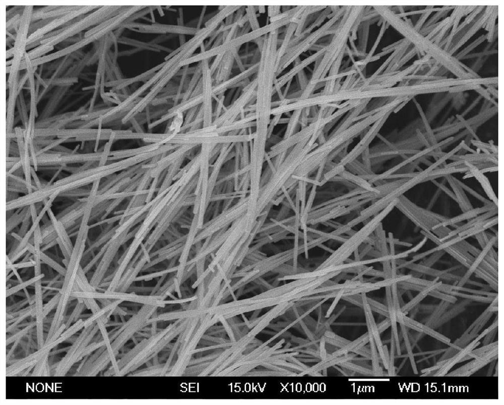
Preparation method of out-phase junction CdS nanowire
A nanowire and heterophase technology, applied in the field of preparation of heterojunction CdS nanowires, can solve the problems of insufficient performance, high cost, complex preparation route, etc., and achieve photocatalytic degradation efficiency and piezoelectric photocatalytic degradation efficiency. The effect of improving the photocatalytic degradation efficiency and piezoelectric photocatalytic degradation efficiency, and the preparation method is simple
- Summary
- Abstract
- Description
- Claims
- Application Information
AI Technical Summary
Problems solved by technology
Method used
Image

Examples
preparation example Construction
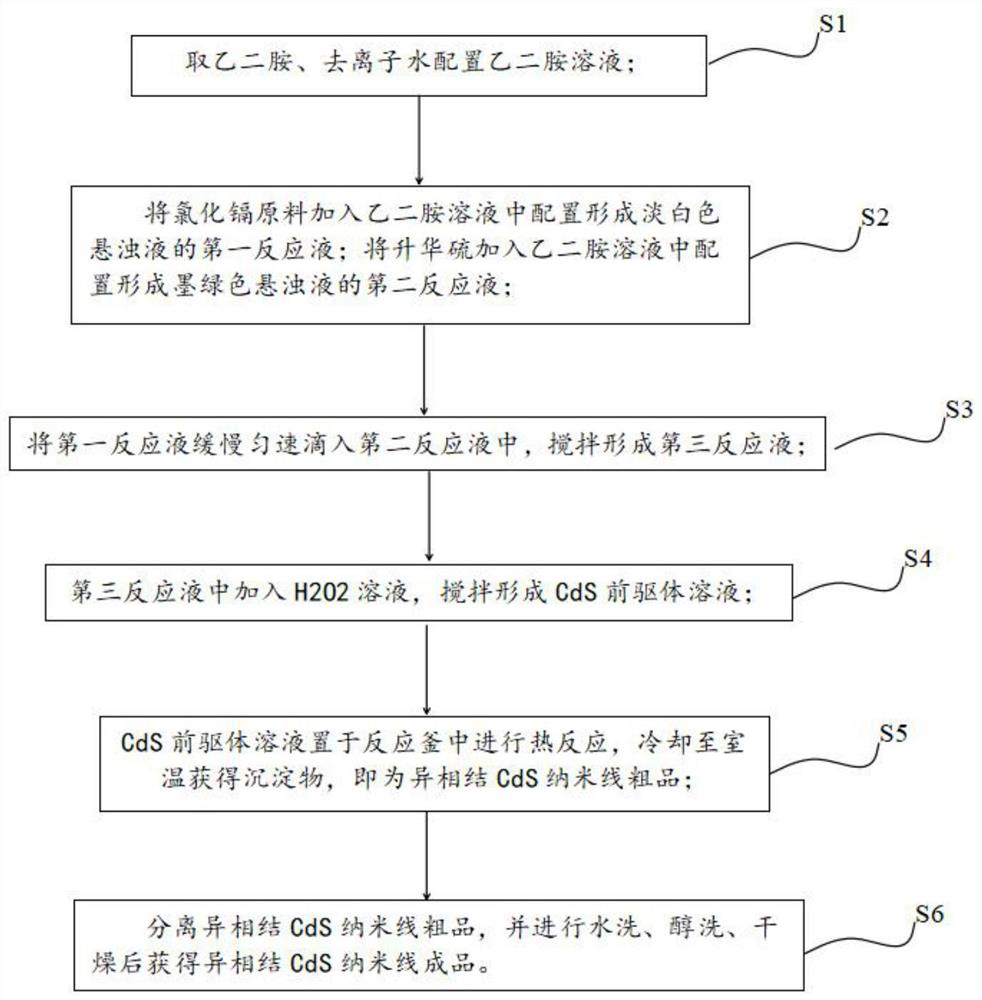
[0040] This specific embodiment also provides the preparation method of the above-mentioned heterogeneous junction CdS nanowire, such as figure 2 shown, including the following steps:
[0041] S1. Take ethylenediamine and deionized water to prepare an ethylenediamine solution.
[0042] In this step, the volume ratio between ethylenediamine and deionized water is 9:1.
[0043] S2. Adding the cadmium chloride raw material to the ethylenediamine solution to form a first reaction solution of a pale white suspension; adding sublimated sulfur to the ethylenediamine solution to form a second reaction solution of a dark green suspension.
[0044] In this step, the mass of the cadmium chloride prepared in the first reaction liquid is 0.077-0.462 g, and the mass of the sublimed sulfur prepared in the second reaction liquid is 0.0213-0.128 g. When configuring the first reaction solution and the second reaction solution, add the solute into the ethylenediamine solution and stir for abo...
example 1
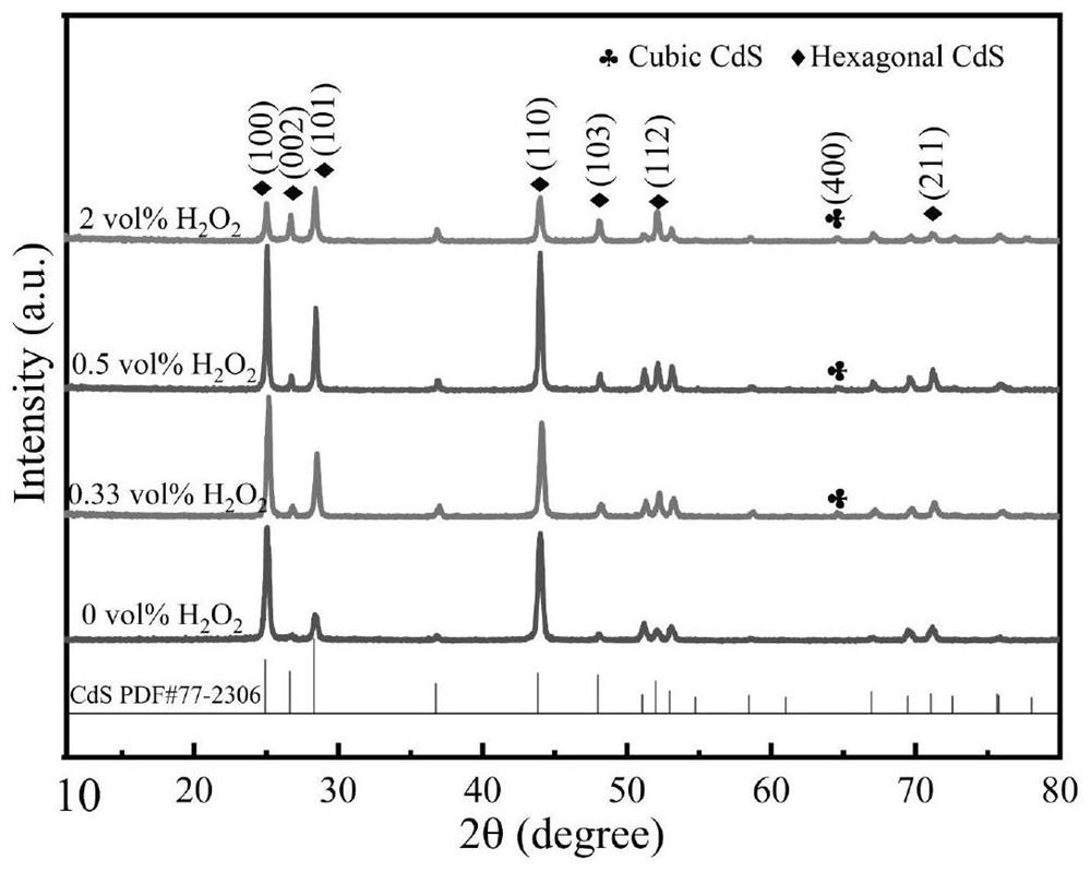
[0063] Example 1 is a comparative example, in the process of preparing the CdS precursor solution, no H 2 o 2 solution.
[0064] The process of preparing heterogeneous junction CdS nanowires is as follows:
[0065] First, measure 13.5mL of ethylenediamine and 1.5mL of deionized water, and mix them evenly to form an ethylenediamine solution;
[0066] Next, take by weighing 0.231g cadmium chloride and 0.064g sublimated sulfur, be dissolved in ethylenediamine solution respectively, stir for 30min to obtain the first reaction solution of light white suspension and the second reaction solution of dark green suspension;
[0067] Once again, slowly drop the first reaction solution into the second reaction solution with a burette or dropper and mix thoroughly, the solution gradually changes from dark green to green, and stirs again for 30 minutes until the solution turns yellow to obtain the third reaction solution (i.e. is the CdS precursor solution of this example);
[0068] The...
example 2
[0071] The process of preparing heterogeneous junction CdS nanowires is as follows:
[0072] First, measure 13.5mL of ethylenediamine and 1.5mL of deionized water, and mix them evenly to form an ethylenediamine solution;
[0073] Next, take by weighing 0.231g cadmium chloride and 0.064g sublimated sulfur, be dissolved in ethylenediamine solution respectively, stir for 30min to obtain the first reaction solution of light white suspension and the second reaction solution of dark green suspension;
[0074] Again, use a burette or dropper to slowly drop the first reaction solution into the second reaction solution and mix thoroughly, the solution gradually turns from dark green to green, and stir again for 30 minutes until the solution turns yellow to obtain the third reaction solution;
[0075] Then, add H to the third reaction solution with a microsyringe 2 o 2 Solution (H 2 o 2 The volume ratio of the solution to the third reaction solution is 0.33%), stirring for 30min to ...
PUM
 Abstract
Description
Claims
Application Information