Semiconductor laser based on distributed phase compensation technology

A phase compensation and semiconductor technology, which is applied in the field of optoelectronics, can solve problems such as poor single-mode characteristics of lasers and unstable output modes of lasers, and achieve the effect of improving lasing modes, increasing energy utilization and output power, and realizing phase compensation.

Pending Publication Date: 2022-01-28
南京华飞光电科技有限公司
View PDF0 Cites 0 Cited by
  • Summary
  • Abstract
  • Description
  • Claims
  • Application Information

AI Technical Summary

Problems solved by technology

However, the reflection phase of the end face introduced by the highly reflective coating is random and fluctuates in the range of 0-2π according to the thickness of the coating. When the reflection phase of the end face is near π, the laser can achieve good single-mode lasing, and if the end face If the reflection phase is close to 0 or 2π, the single-mode characteristic of the laser will be relatively poor
Therefore, the randomness of this coating thickness will bring great instability to the output mode of the laser

Method used


Image

  • Semiconductor laser based on distributed phase compensation technology
  • Semiconductor laser based on distributed phase compensation technology
  • Semiconductor laser based on distributed phase compensation technology

Examples


Embodiment

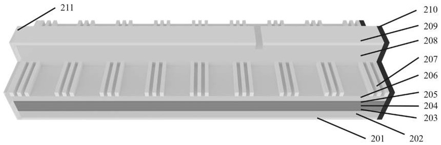
[0036] Taking the operating wavelength within the range of 1550nm as an example, a semiconductor laser based on distributed phase compensation technology provided by the present invention is described below, and the preparation process of the semiconductor laser is specifically as follows:

[0037] (1) First, the epitaxial material is manufactured by MOVPE technology, and the n-type InP buffer layer (thickness 200nm, doping concentration about 1.1x10 18 cm -2 ), non-doped lattice-matched InGaAsP confinement layer (thickness 100nm), strained InGaAsP multi-quantum well layer (fluorescence wavelength 1.52 microns, 7 quantum wells: well width 8nm, 0.5% compressive strain, barrier width 10nm, lattice matching material), p-type lattice matching InGaAsP (thickness 100nm, doping concentration about 1.1x10 17 cm -2 ) on the confinement layer and corrosion barrier layer respectively;

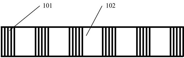
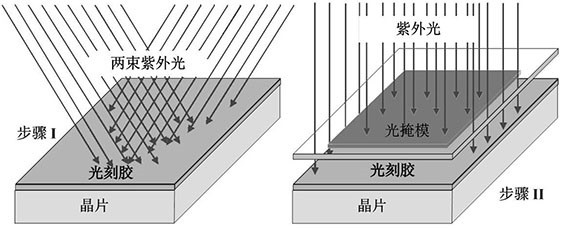
[0038] (2) Design and manufacture the sampling grating pattern of semiconductor lasers based on dis...


PUM

PropertyMeasurementUnit
widthaaaaaaaaaa
lengthaaaaaaaaaa
reflectanceaaaaaaaaaa

Abstract

The invention discloses a semiconductor laser based on a distributed phase compensation technology, and relates to the field of optical fiber communication and photon integration. The semiconductor laser comprises a metal n electrode, a buffer layer, a lower respective limiting layer, a light-emitting active layer, an upper respective limiting layer, a corrosion barrier layer, a grating layer, a waveguide layer, a transition layer, a p-type ohmic contact layer, a metal p electrode, a high-reflection film and an anti-reflection film. The high-reflection film and the anti-reflection film are arranged at the two ends of the semiconductor laser respectively, so that the energy utilization rate and the output power of the semiconductor laser are improved; and electrical isolation is formed by etching the waveguide, the semiconductor laser is divided into two or more sections, and the current injection distribution of each section is changed, so that the random reflection phase brought by the high-reflection coating can be effectively compensated, the problem of unstable lasing mode caused by the random reflection phase is solved, and the micro regulating and control of wavelength can be realized.

Description

technical field [0001] The invention belongs to the field of optoelectronic technology, relates to the fields of optical fiber communication and photon integration, and in particular relates to a semiconductor laser based on distributed phase compensation technology. Background technique [0002] In recent decades, optical communication technology has developed very rapidly, and has become the mainstream transmission method in many aspects. Its advantages are mainly reflected in: 1. The bandwidth of light is very high, that is, the information transmission capacity is large; 2. The transmission loss of light in the optical fiber is very low, especially for long-distance transmission. The advantages of optical fiber are more obvious, and the cost is low. Lightweight, strong anti-interference ability; Third, thanks to the development of semiconductor lasers, the manufacturing difficulty and cost of the core components of optical communication light sources and photodetectors h...

Claims


Application Information

Patent Timeline
Patent Type & Authority Applications(China)
IPC IPC(8): H01S5/12H01S5/042H01S5/028
CPCH01S5/1209H01S5/1215H01S5/124H01S5/04256H01S5/04254H01S5/028
Inventor 吕根周亚亭肖如磊樊荣虎陈向飞
Owner 南京华飞光电科技有限公司
Why Eureka
Try Eureka