Super-hydrophobic digital micro-fluidic chip based on anodic oxidation method, manufacturing method thereof, and liquid drop control system

An anodic oxidation method and digital microfluidic technology, applied in fluid controllers, chemical instruments and methods, and laboratory containers, can solve problems such as high driving voltage, high cost, and complicated preparation methods, and reduce motion resistance , Simple preparation, and the effect of driving voltage

Active Publication Date: 2022-02-01
HARBIN INST OF TECH
View PDF18 Cites 1 Cited by
  • Summary
  • Abstract
  • Description
  • Claims
  • Application Information

AI Technical Summary

Problems solved by technology

[0004] The purpose of the present invention is to solve the problem that the existing hydrophobic digital microfluidic chip has complex preparation methods, high cost, and requires a high driving voltage to control the movement of droplets. The present invention proposes a superhydrophobic digital microfluidic chip Flow control chip and its manufacturing method

Method used


Image

  • Super-hydrophobic digital micro-fluidic chip based on anodic oxidation method, manufacturing method thereof, and liquid drop control system
  • Super-hydrophobic digital micro-fluidic chip based on anodic oxidation method, manufacturing method thereof, and liquid drop control system
  • Super-hydrophobic digital micro-fluidic chip based on anodic oxidation method, manufacturing method thereof, and liquid drop control system

Examples


specific Embodiment approach 1

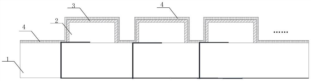
[0038] Specific implementation mode one: the following combination figure 1 Describe this embodiment, a super-hydrophobic digital microfluidic chip based on the anodic oxidation method described in this embodiment, the super-hydrophobic digital microfluidic chip includes a first substrate 1, an electrode sheet 2, and a first dielectric layer 3 and the first hydrophobic layer 4;

[0039] The top surface of the first substrate 1 is covered with a plurality of electrode sheets 2, and the plurality of electrode sheets 2 are in an array covering the top surface of the first substrate 1, and the body of the first substrate 1 is provided with a plurality of through holes. The plurality of through holes correspond to the electrode sheets 2 one by one;

[0040] The bottom surface of the first substrate 1 is provided with a plurality of wires, and each wire is connected to a through hole; each wire is electrically connected to an electrode sheet 2 through a through hole process;

[00...

specific Embodiment approach 2

[0046] Specific embodiment 2. This embodiment describes a method for manufacturing a super-hydrophobic digital microfluidic chip based on the anodic oxidation method described in specific embodiment 1, including:

[0047] Step 1. The electrode sheet 2 and the wires are respectively arranged on both sides of the first substrate 1 by using the PCB preparation process, and the wires are connected to the electrode sheet 2 through the via hole process, and the via holes are sealed by the via hole capping oil process;

[0048] Step 2, covering the electrode sheet 2 with a dielectric layer by anodic oxidation;

[0049] Step 3: Soak the first substrate 1 covered with the dielectric layer in a hydrophobic reagent to prepare a hydrophobic layer, and complete the manufacture of a super-hydrophobic digital microfluidic chip.

[0050] Further, in this embodiment, in step 2, the specific method of covering the electrode sheet 2 with a dielectric layer by anodic oxidation is as follows:

[...

specific Embodiment approach 3

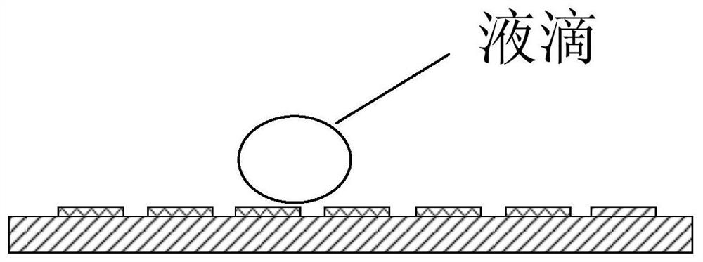
[0060] Embodiment 3: This embodiment is based on the drip control system based on the super-hydrophobic digital microfluidic chip described in Embodiment 1. It is divided into a single-layer drive mode and a double-layer drive mode. The single-layer drive mode is based on the bottom plate Chip implementation, also including a microprocessor and multiple relays;

[0061] A relay is connected between each wire connected to the bottom layer of the superhydrophobic digital microfluidic chip wiring and the power supply, and the switch control signal input end of each relay is connected to a switch control signal output end of the microcontroller;

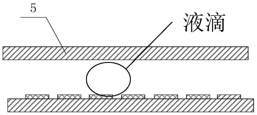
[0062] The double-layer driving mode is realized based on the bottom board chip, and also includes a microprocessor, top board chip 5 and multiple relays;

[0063] The top plate chip 5 includes a second substrate, a second electrode layer and a second hydrophobic layer;

[0064] The second electrode layer covers one side of the second s...


PUM


Abstract

The invention discloses a super-hydrophobic digital micro-fluidic chip based on an anodic oxidation method, a manufacturing method thereof, and a liquid drop control system, and relates to the field of biochemical detection micro-fluidic chips. The problems that an existing hydrophobic digital micro-fluidic chip is complex in preparation mode and high in manufacturing cost, and liquid drops can be controlled to move only by high driving voltage are solved. The top surface of a first substrate of the super-hydrophobic digital micro-fluidic chip is covered with a plurality of electrode plates, the plurality of electrode plates are distributed on the top surface of the first substrate in an array manner, the plate body of the first substrate is provided with a plurality of through holes, and the plurality of through holes are in one-to-one correspondence with the electrode slices; a plurality of wires are distributed on the bottom surface of the first substrate, and each wire is connected with one through hole; each lead is electrically connected with one electrode plate through a via hole process; and the outer side of each electrode plate is covered with a first dielectric layer, the upper surfaces of the first dielectric layers and the upper surface of the first substrate are both covered with hydrophobic layers, and the first dielectric layers are prepared by anodizing the electrode plates in an alkaline solution. The chip is suitable for biochemical detection microfluidics.

Description

technical field [0001] The invention relates to the field of biochemical detection microfluidic chips. Background technique [0002] The digital microfluidic chip uses dielectric wetting technology to manipulate and control micro-droplets, realizing the detection function of large-scale equipment in traditional laboratories. Because of its high throughput, low fluid consumption, and rapid detection capabilities, it has broad development prospects in the field of medical testing. However, the current method of preparing digital microfluidic chips is mainly through photolithography on conductive glass, or magnetron detection on the substrate to form a dense microelectrode array, and then spin-coat a dielectric layer on this basis. The preparation method is complicated and the cost is high, and it cannot be mass-produced on a large scale, and it is difficult to be used for large-scale biochemical detection in the future. [0003] Printed circuit board (PCB) is a very mature c...

Claims


Application Information

Patent Timeline
Patent Type & Authority Applications(China)
IPC IPC(8): B01L3/00
CPCB01L3/50273B01L3/502707B01L2200/0605B01L2200/0636B01L2200/143B01L2300/0861B01L2300/0887B01L2300/166B01L2400/0427
Inventor 陈亮梁昊付强姜舒月刘晓为张海峰曹伽牧
Owner HARBIN INST OF TECH
Why Eureka
Try Eureka