
Low-cost stable wafer-level metal diffusion bonding method and semiconductor wafer

A metal diffusion, low-cost technology, applied in the field of electronic science, can solve the problems of Cu or Al fracture, affect the bonding efficiency, easy to form oxide layer, etc., achieve the effect of reducing usage, good bonding effect, and promoting diffusion

Pending Publication Date: 2022-02-08
SUZHOU INST OF NANO TECH & NANO BIONICS CHINESE ACEDEMY OF SCI
View PDF0 Cites 0 Cited by
  • Summary
  • Abstract
  • Description
  • Claims
  • Application Information

AI Technical Summary

Problems solved by technology

However, in order to increase the bonding rate, the thickness of the Au film has to be increased, thereby increasing its cost
[0005] Although the cost of Cu-Cu bonding and Al-Al bonding is low, after Cu or Al is deposited, an oxide layer is easily formed on its surface, which seriously affects the bonding efficiency. Secondly, vapor phase bonding is used during bonding. The high pressure used in the cleaning process to remove surface oxides will cause fracture of Cu or Al, and its bonding temperature is high

Method used


Image

  • Low-cost stable wafer-level metal diffusion bonding method and semiconductor wafer
  • Low-cost stable wafer-level metal diffusion bonding method and semiconductor wafer
  • Low-cost stable wafer-level metal diffusion bonding method and semiconductor wafer

Examples


Embodiment 1

[0071] In this embodiment, two Si chips are bonded, which can be used for experimental verification before formal chip bonding.

[0072] A low-cost and stable wafer-level metal diffusion bonding method, comprising the following steps:

[0073] Step 1: Substrate acquisition and cleaning

[0074] Organic cleaning: First place two four-inch Si wafers in acetone solution for ultrasonic cleaning for 10 minutes, then ultrasonically clean them in isopropanol solution for 10 minutes, then put them in ultrapure water for ultrasonic cleaning for 5 minutes, and rinse with ultrapure water repeatedly to remove residues Acetone and isopropanol solutions, finally blown dry with nitrogen to remove surface organics;

[0075] Inorganic cleaning: Put two four-inch Si wafers in HF:H 2 Soak in O=1:10 solution for 1min to remove surface oxides;

[0076] Step 2: Dielectric Layer Deposition

[0077] Deposit 500nm SiN on cleaned Si wafer in PECVD system x A dielectric layer to prevent the diffusi...

Embodiment 2

[0085] This embodiment can be used in the preparation of vertical GaN-based LEDs.

[0086] A method for preparing a vertical GaN-based LED, comprising the steps of:

[0087] Step 1: Wafer Acquisition and Cleaning

[0088] Organic cleaning: first place the GaN-based LED and Si chip with ohmic contact on the sapphire substrate in an acetone solution for 10 minutes of ultrasonic cleaning, then in an isopropanol solution for 10 minutes, and then put it into ultrapure water for 5 minutes of ultrasonic cleaning , rinse with ultrapure water repeatedly to remove residual acetone and isopropanol solutions, and finally dry with nitrogen to remove surface organic matter;

[0089] Step 2: Deposit metal adhesion layer, diffusion barrier layer, deformation layer and passivation layer in sequence

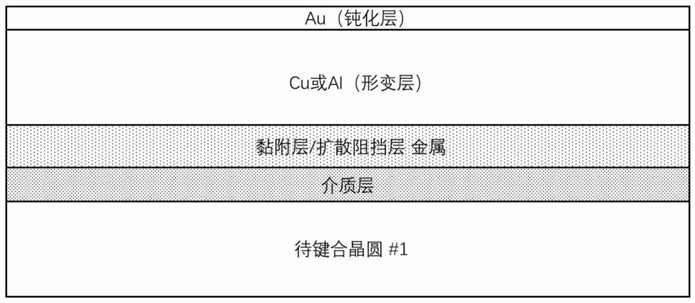
[0090] Using magnetron sputtering technology, the GaN-based LED and the Si wafer are sequentially sputtered to form a Ti metal adhesion layer / TiW diffusion barrier layer / Al deformation layer / Au ...

Embodiment 3

[0096] A method for preparing N-polar GaN based on a substrate lift-off method, comprising the steps of:

[0097] Step 1: Wafer Acquisition and Cleaning

[0098] Organic cleaning: first place Ga-polar GaN epitaxial wafers and Si wafers based on Si substrates in acetone solution for 10 minutes, then ultrasonically clean them in isopropanol solution for 10 minutes, then put them into ultrapure water for 5 minutes, and use them repeatedly Rinse with ultrapure water to remove residual acetone and isopropanol solutions, and finally blow dry with nitrogen to remove surface organic matter;

[0099] Inorganic cleaning: soak Ga-polar GaN epitaxial wafers based on Si substrates in HCl:H 2 O 1:5 solution for 2min to remove surface oxides; place Si sheet in HF:H 2 Soak in O=1:10 solution for 1min to remove surface oxides;

[0100] Step 2: Dielectric Layer Deposition

[0101] In the PECVD system, 400nm SiO was deposited on the cleaned Ga-polar GaN epitaxial wafer and Si wafer. 2 Diele...


PUM

PropertyMeasurementUnit
thicknessaaaaaaaaaa
thicknessaaaaaaaaaa
thicknessaaaaaaaaaa

Abstract

The invention discloses a low-cost stable wafer-level metal diffusion bonding method and a semiconductor wafer. The wafer-level metal diffusion bonding method comprises the steps of forming a first bonding metal layer on a first surface of a first wafer, wherein the first bonding metal layer comprises first deformation layer metal and first passivation layer metal; forming a second bonding metal layer on the second surface of the second wafer, wherein the second bonding metal layer comprises second deformation layer metal and second passivation layer metal; and at least performing plasma surface activation treatment on the first passivation layer metal and the second passivation layer metal to attach the first bonding metal layer and the second bonding metal layer, and at least enabling the first passivation layer metal and the second passivation layer metal to be combined into a whole in a thermocompression bonding mode. According to the wafer-level metal diffusion bonding method provided by the embodiment of the invention, the problem of surface oxidation of the Al-Al or Cu-Cu bonding metal layer is solved, and the bonding temperature is reduced.

Description

technical field [0001] The invention relates to a wafer bonding method, in particular to a low-cost and stable wafer-level metal diffusion bonding method and a semiconductor wafer, belonging to the field of electronic science and technology. Background technique [0002] In recent years, semiconductor packaging technology is entering the era of three-dimensional stacking from the original two-dimensional packaging, and is developing in the direction of low cost, high performance, high integration, small size, and low power consumption. In the packaging process of semiconductor devices and integrated circuits, wafer-level bonding technology plays an important role. More than half of the packaging technology uses the wafer-level bonding process. In addition to being widely used in advanced packaging processes, the wafer-level bonding process is also used in the packaging and manufacturing of MEMS devices, and the substrate transfer of high-brightness LEDs. , CMOS image sensor...

Claims


Application Information

Patent Timeline
Patent Type & Authority Applications(China)
IPC IPC(8): H01L21/603H01L23/488
CPCH01L24/83H01L24/29H01L2224/83009H01L2224/83203H01L2224/29082H01L2224/29124H01L2224/29144H01L2224/29147
Inventor 张丽于子呈姜春宇于国浩张宝顺
Owner SUZHOU INST OF NANO TECH & NANO BIONICS CHINESE ACEDEMY OF SCI
Learn More