Preparation method of vanadium dioxide film
A vanadium dioxide and thin film technology, applied in metal material coating process, vacuum evaporation coating, coating and other directions, can solve the problems of high cost, complex method, complex preparation process, etc., to ensure crystallinity, high infrared mutation Amplitude, easy operation effect
- Summary
- Abstract
- Description
- Claims
- Application Information
AI Technical Summary
Problems solved by technology
Method used
Image
Examples
preparation example Construction
[0033] The invention provides a kind of preparation method of vanadium dioxide film, comprises the following steps:
[0034] In a vacuum reaction chamber, radio frequency magnetron sputtering is used to sputter vanadium dioxide on the surface of the substrate, and the temperature of the substrate is increased to perform in-situ annealing to obtain a vanadium dioxide film; there is no gap between the substrate and the vanadium dioxide film. set the buffer layer;
[0035] The conditions of the radio frequency magnetron sputtering are: the temperature of the substrate is 250-300° C.; the flow rate of argon into the reaction chamber is 0.8 sccm; the flow rate of oxygen into the reaction chamber is 40 sccm; the pressure of the reaction chamber is 0.8 Pa; sputtering time is 15-20min; sputtering power is 95W;
[0036] The temperature of the in-situ annealing is 460-520°C, and the holding time is 200s;
[0037] The time for heating up to the temperature of the in-situ annealing is ≤...
Embodiment 1
[0059] The sapphire substrate was ultrasonically cleaned with acetone, absolute ethanol and high-purity deionized water for 15 minutes, then dried with a nitrogen gun and placed in a sputtering chamber;
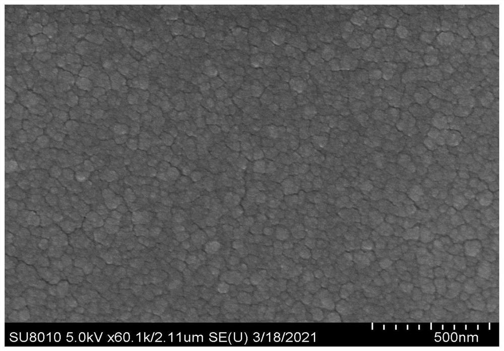
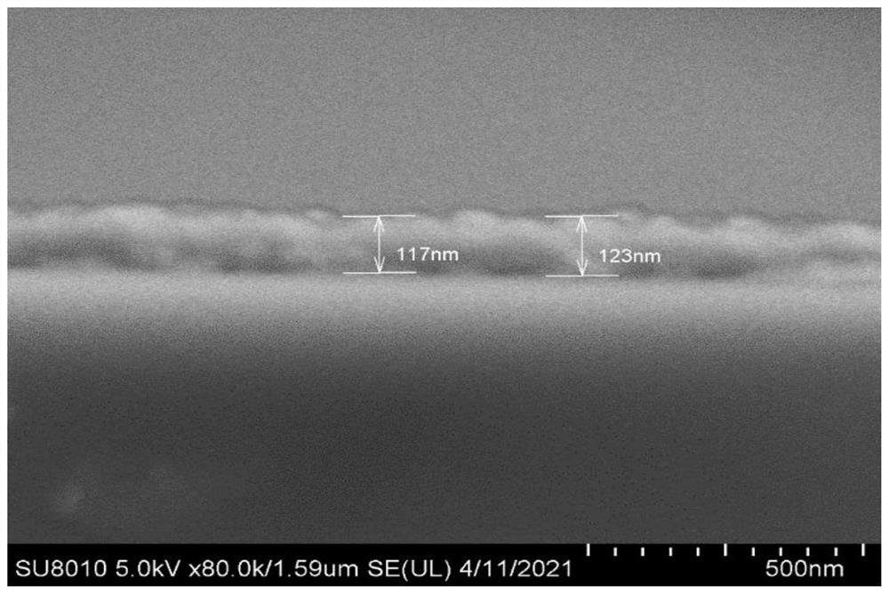
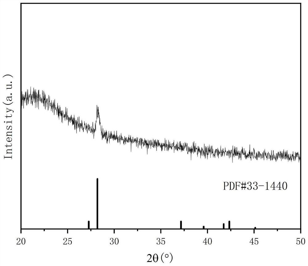
[0060] Pump the pressure in the sputtering chamber to 8×10 through a mechanical pump -4 Pa, raise the substrate temperature to 270°C, control oxygen and argon to flow into the reaction chamber at a flow rate of 0.8sccm and 40sccm through the gas flow meter, and control the sputtering pressure to 0.8Pa through the gate valve; use the baffle Put on the target, turn on the sputtering power supply for pre-sputtering (sputtering power is 95W), to remove impurities on the surface of the target; remove the baffle, set the distance between the target and the substrate to 80mm, the substrate speed to 25rad / s, radio frequency The power is 95W, after deposition for 16min, turn off the gas flowmeter, heat the substrate temperature to 490°C for 7s, keep it warm for 200s, and cool it to ro...
PUM
| Property | Measurement | Unit |
|---|---|---|
| thickness | aaaaa | aaaaa |
| thickness | aaaaa | aaaaa |
| thickness | aaaaa | aaaaa |
Abstract
Description
Claims
Application Information


