Solar cell and cell module

A technology of solar cells and conductive layers, applied in the field of solar cells, to achieve the effects of simplifying the process, improving conversion efficiency, and reducing difficulty

Pending Publication Date: 2022-02-18
ZHEJIANG AIKO SOLAR ENERGY TECH CO LTD +3
View PDF0 Cites 0 Cited by
  • Summary
  • Abstract
  • Description
  • Claims
  • Application Information

AI Technical Summary

Problems solved by technology

[0005] The embodiment of the present application provides a solar cell and a cell module, aiming to solve the problem of how t

Method used


Image

  • Solar cell and cell module
  • Solar cell and cell module
  • Solar cell and cell module

Examples


Embodiment 1

[0039] In the present application, a solar cell is provided, and only the portion related to the present application embodiment is shown in order to facilitate explanation.

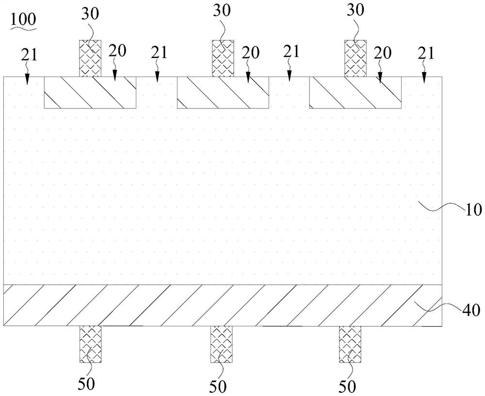
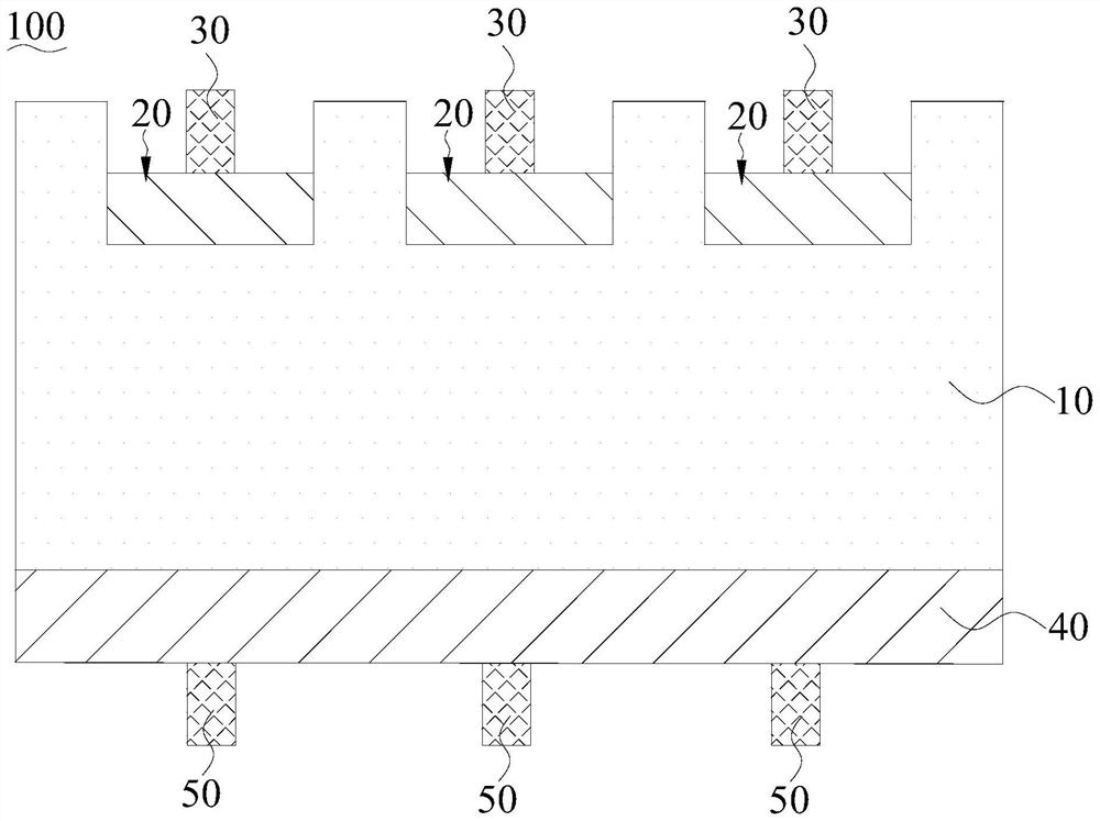
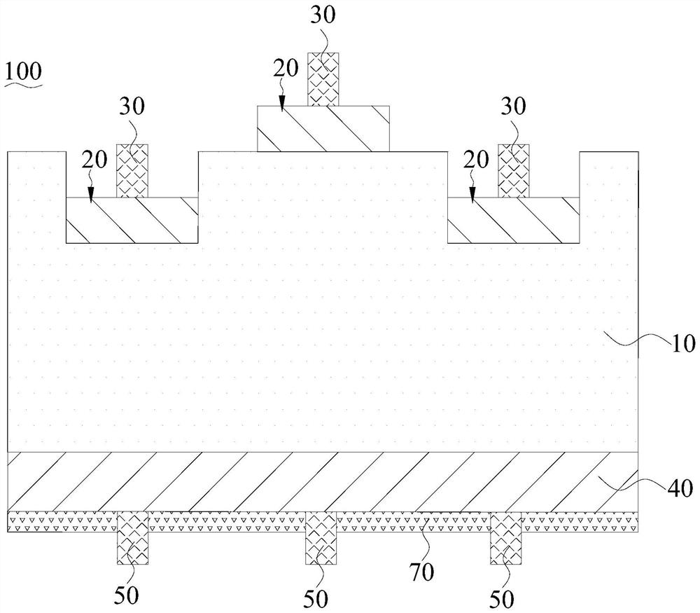
[0040] See figure 1 The solar cell 100 provided by the present application embodiment includes: silicon substrate 10, in which the first doped region 20 and the first conductive layer 30 are sequentially provided in the back surface of the silicon substrate 10. The back passivation contact structure 40 and the second conductive layer 50; the number of the first doped regions 20 is a plurality of first doped regions 20, and the doped polarity and silicon lining of the first doped region 20 is intervals. The polarity of the bottom 10 is the same, and the first conductive layer 30 is electrically contacted with the first doping region 20, and the second conductive layer 50 is electrically contacted with the back surface passivation contact structure 40.

[0041] The solar cell 100 of the present application embo...

Embodiment 2

[0128] The second embodiment of this application also provides a battery assembly comprising the solar cell 100 of the foregoing embodiment one.

[0129] The battery assembly of the second embodiment of the present application, since the solar cell 100 is the same as the first doped region 20 having the same polarity in the silicon substrate, most carriers can be transmitted through the body region of the silicon substrate 10 to the first A doped region 20, so that the first doped region 20 does not need to contact the silicon substrate 10, thereby reducing the Russian compound brought by using a diffusion process, or can reduce the passivation contact structure as a Parasitic absorption brought by a front surface field. At the same time, this can be adapted to the quality of the quality of the silicon substrate 10, which utilizes the advantages of high quality of the silicon substrate, so that the body region of the silicon substrate 10 is more fully transported, which is advanta...


PUM

PropertyMeasurementUnit
Heightaaaaaaaaaa
Apertureaaaaaaaaaa
Thicknessaaaaaaaaaa

Abstract

The invention is suitable for the technical field of solar cells, and provides a solar cell and a cell module, and the solar cell comprises a silicon substrate, a first doped region and a first conductive layer which are sequentially disposed on the front surface of the silicon substrate, and a back passivation contact structure and a second conductive layer which are sequentially disposed on the back surface of the silicon substrate. Multiple first doped regions are mutually spaced, the doping polarity of the first doped regions is the same with the polarity of the silicon substrate, the first conductive layer is in electric contact with the first doped regions, and the second conductive layer is in electric contact with the back passivation contact structure. Thus, due to the fact that the first doped regions with the same polarity as the silicon substrate are locally designed, most carriers can be transmitted to the first doped regions through the body region of the silicon substrate, the first doped regions do not need to make contact with the whole surface of the silicon substrate, and auger recombination or parasitic absorption can be reduced. Meanwhile, the body region of the silicon substrate can transport carriers more sufficiently.

Description

Technical field [0001] The present application belongs to the field of solar cell technology, and in particular, there is a solar cell and a battery assembly. Background technique [0002] The electricity of solar cells is a sustainable source source. The solar cell utilizes the semiconductor P-N junction can convert the sunlight into electrical energy, so the photoelectric conversion efficiency is an important indicator for measuring the performance of solar cell. In solar cells, loss of photoelectric conversion efficiency includes two aspects of electrical loss and optical losses. Electrical loss mainly includes a composite loss and resistance loss caused by metal-semiconductor contact, and optical losses mainly include occlusion of the light grating line. [0003] The double-sided contact back tuning solar cell in the related art is typically designed as the entire surface of the emitter and the surface field to carry out the transmission of carriers to reduce electrical loss ...

Claims


Application Information

Patent Timeline
IPC IPC(8): H01L31/0352H01L31/068
CPCH01L31/03529H01L31/068Y02E10/547
Inventor 邱开富林文杰许文理王永谦陈刚
Owner ZHEJIANG AIKO SOLAR ENERGY TECH CO LTD
Why Eureka
Try Eureka