Semiconductor structure and preparation method thereof

A technology of semiconductor and conductive structure, applied in the field of semiconductor structure and its preparation, can solve the problems of breakdown, high on-current, increased leakage, etc., and achieve the effects of improving performance, improving conductivity, and avoiding leakage

Pending Publication Date: 2022-02-22
CHANGXIN MEMORY TECH INC
View PDF0 Cites 1 Cited by
  • Summary
  • Abstract
  • Description
  • Claims
  • Application Information

AI Technical Summary

Problems solved by technology

For the array area, the thicker the transition layer, the greater the conduction current and the better the performance of the wire. For the peripheral circuit area, if the transition layer is too thick, it will cause too high a conduction current, which may cause Breakdown effect, resulting in increased leakage

Method used


Image

  • Semiconductor structure and preparation method thereof
  • Semiconductor structure and preparation method thereof
  • Semiconductor structure and preparation method thereof

Examples


Embodiment Construction

[0027] Specific implementations of the semiconductor structure and its preparation method provided by the present invention will be described in detail below in conjunction with the accompanying drawings.

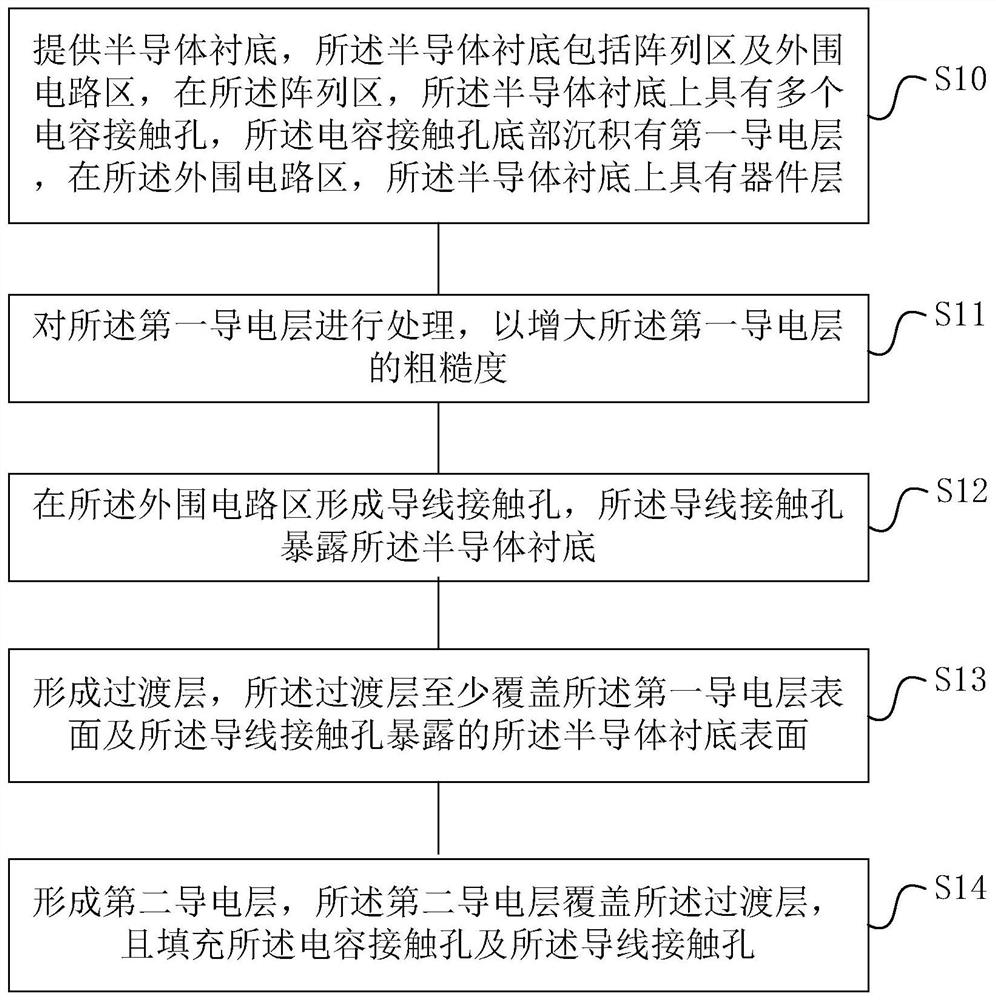
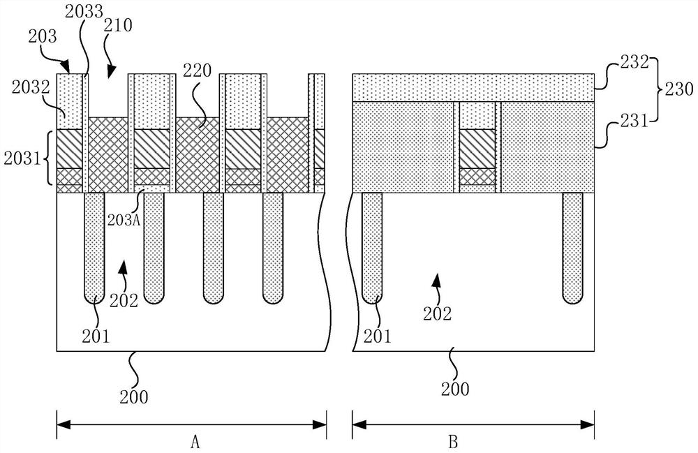
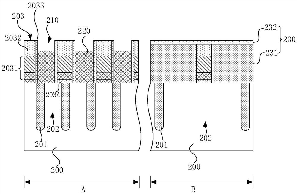
[0028] figure 1 It is a schematic diagram of the steps of an embodiment of the method for preparing a semiconductor structure of the present invention. see figure 1 , the preparation method of the semiconductor structure includes the following steps: Step S10, providing a semiconductor substrate, the semiconductor substrate includes an array area and a peripheral circuit area, and in the array area, the semiconductor substrate has a plurality of capacitive contacts hole, the bottom of the capacitive contact hole is deposited with a first conductive layer, and in the peripheral circuit area, there is a device layer on the semiconductor substrate; step S11, processing the first conductive layer to increase the The roughness of the first conductive layer; step S12, forming a...


PUM


Abstract

The invention provides a semiconductor structure and a preparation method thereof. the preparation method comprises the following steps: providing a semiconductor substrate which comprises an array region and a peripheral circuit region, wherein the array region and the semiconductor substrate are provided with a plurality of capacitor contact holes, the bottoms of the capacitor contact holes are provided with first conductive layers, and in the peripheral circuit region, a device layer is arranged on the semiconductor substrate; processing the first conductive layer to increase the roughness of the first conductive layer; forming a wire contact hole in the peripheral circuit area, wherein the wire contact hole exposes the semiconductor substrate; forming a transition layer, wherein the transition layer at least covers the surface of the first conductive layer and the surface of the semiconductor substrate exposed by the wire contact hole; and forming a second conductive layer which covers the transition layer and fills the capacitor contact hole and the wire contact hole. Transition layers with different thicknesses can be formed in the array area and the peripheral circuit area, and the performance of the semiconductor structure is greatly improved.

Description

technical field [0001] The invention relates to the field of semiconductor manufacturing, in particular to a semiconductor structure and a preparation method thereof. Background technique [0002] Dynamic Random Access Memory (Dynamic Random Access Memory, DRAM) is a common semiconductor memory device in computers, and its memory array area is composed of many repeated memory cells. Each memory cell usually includes a capacitor and a transistor. The gate of the transistor is connected to the bit line structure, one of the drain or source is connected to the bit line structure, and one of the drain or source is connected to the capacitor. On the bit line structure The voltage signal can control the opening or closing of the transistor, and then read the data information stored in the capacitor through the bit line structure, or write the data information into the capacitor through the bit line structure for storage. [0003] With the shrinking of the manufacturing process, t...

Claims


Application Information

Patent Timeline
IPC IPC(8): H01L21/8242H01L27/108
CPCH10B12/30H10B12/09H10B12/50H01L29/78H10B12/00
Inventor 卢经文朱柄宇白世杰
Owner CHANGXIN MEMORY TECH INC
Why Eureka
Try Eureka