High-uniformity and high-power laser epitaxial wafer and preparation method thereof

A technology of lasers and epitaxial wafers, applied in the field of optoelectronics, can solve the problems of great influence of temperature, poor wavelength uniformity of epitaxial wafers, carrier leakage, etc., and achieve the effect of improving growth quality

Pending Publication Date: 2022-02-22
Shandong Huaguang Optoelectronics Co. Ltd.
View PDF0 Cites 0 Cited by
  • Summary
  • Abstract
  • Description
  • Claims
  • Application Information

AI Technical Summary

Problems solved by technology

[0005] For the aluminum-free material structure, although it has the above advantages, due to the small heterojunction band order of the quantum well layer and the barrier and the upper confinement layer, the insufficient confinement capacity will cause carrier leakage, resulting in an increase in the threshold current density of the device. Efficiency drops and temperature characteristics deteriorate
In actual commercial production, since the temperature field distribution in the reaction chamber of MOCVD equipment is not uniform, and the ratio of As and P in the GaAsP material is greatly affected by temperature, although GaAsP is used as a quantum well material, it can be obtained in terms of reliability. However, due to the influence of the temperature field, the wavelength uniformity of the 808nm semiconductor laser epitaxial wafer of the actually grown GaAsP quantum well is very poor, and due to the temperature fluctuation between furnaces, the proportion of As and P in the GaAsP material It is also changing, and the actual wavelength of the epitaxial wafer is also affected by it, so it is very difficult to stabilize mass production

Method used


Image

  • High-uniformity and high-power laser epitaxial wafer and preparation method thereof
  • High-uniformity and high-power laser epitaxial wafer and preparation method thereof
  • High-uniformity and high-power laser epitaxial wafer and preparation method thereof

Examples


Embodiment 1

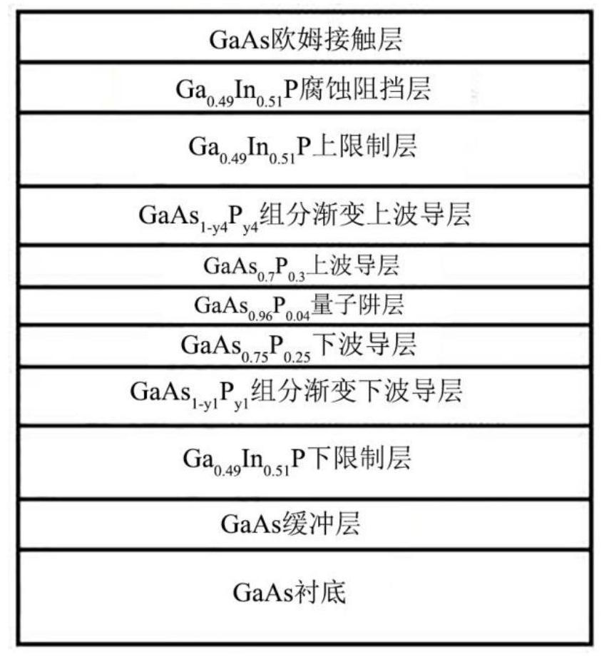
[0051] A high-uniformity high-power laser epitaxial wafer, using a GaAs substrate, on the GaAs substrate from bottom to top includes: GaAs buffer layer, GaAs 0.49 In 0.51 P lower confinement layer, GaAs 1-y1 P y1 Compositionally graded lower waveguide layer, GaAs0.75 P 0.25 Lower waveguide layer, GaAs 0.96 P 0.04 Quantum well layer, GaAs 0.7 P 0.3 Upper waveguide layer, GaAs 1-y4 P y4 Composition-graded upper waveguide layer, Ga 0.49 In 0.51 Confinement layer on P, Ga 0.49 In 0.51 P corrosion barrier layer, GaAs ohmic contact layer; its structure is as figure 1 shown.

[0052] In this example, GaAs 0.75 P 0.25 Lower waveguide layer and GaAs 0.7 P 0.3 The thickness of the upper waveguide layer is 15nm;

[0053] GaAs 1-y1 P y1 The thickness of the waveguide layer is 0.6 μm when the composition is gradually changed; y1 is gradually changed from 0.6 to 0.5;

[0054] GaAs 1-y4 P y4 The thickness of the waveguide layer on the composition gradient is 0.3 μm; y4...

Embodiment 2

[0060] A high-uniformity high-power laser epitaxial wafer adopts a GaAs substrate, and on the GaAs substrate from bottom to top, it includes: a GaAs buffer layer, a GaAs 0.49 In 0.51 P lower confinement layer, GaAs 1-y1 P y1 Compositionally graded lower waveguide layer, GaAs 0.8 P 0.2 Lower waveguide layer, GaAs 0.97 P 0.03 Quantum well layer, GaAs 0.6 P 0.4 Upper waveguide layer, GaAs 1-y4 P y4 Composition-graded upper waveguide layer, Ga 0.49 In 0.51 Confinement layer on P, Ga 0.49 In 0.51 P etch stop layer, GaAs ohmic contact layer.

[0061] In this example, GaAs 0.8 P 0.2 Lower waveguide layer and GaAs 0.6 P 0.4 The thickness of the upper waveguide layer is 18nm;

[0062] GaAs 1-y1 P y1 The thickness of the waveguide layer is 0.6 μm when the composition is gradually changed; y1 is gradually changed from 0.5 to 0.4;

[0063] GaAs 1-y4 P y4 The thickness of the waveguide layer on the composition gradient is 0.3 μm; y4 is gradually changed from 0.5 to 0...

Embodiment 3

[0069] A high-uniformity high-power laser epitaxial wafer adopts a GaAs substrate, and on the GaAs substrate from bottom to top, it includes: a GaAs buffer layer, a GaAs 0.49 In 0.51 P lower confinement layer, GaAs 1-y1 P y1 Compositionally graded lower waveguide layer, GaAs 0.7 P 0.3 Lower waveguide layer, GaAs 0.95 P 0.05 Quantum well layer, GaAs 0.8 P 0.2 Upper waveguide layer, GaAs 1-y4 P y4 Composition-graded upper waveguide layer, Ga 0.49 In 0.51 Confinement layer on P, Ga 0.49 In 0.51 P corrosion barrier layer, GaAs ohmic contact layer; its structure is as figure 1 shown.

[0070] In this example, GaAs 0.7 P 0.3 Lower waveguide layer and GaAs 0.8 P 0.2 The thickness of the upper waveguide layer is 13nm;

[0071] GaAs 1-y1 P y1 The thickness of the waveguide layer is 0.6 μm when the composition is gradually changed; y1 is gradually changed from 0.5 to 0.4;

[0072] GaAs 1-y4 P y4 The thickness of the waveguide layer on the composition gradient is ...


PUM

PropertyMeasurementUnit
thicknessaaaaaaaaaa
thicknessaaaaaaaaaa
thicknessaaaaaaaaaa

Abstract

The invention relates to a high-uniformity and high-power laser epitaxial wafer and a preparation method thereof. An upper waveguide layer and a lower waveguide layer between a GaAsP quantum well and a GaInP limiting layer are each composed of a GaAsP waveguide layer with gradually-changed P components and a GaAsP waveguide layer with fixed components. The GaAsP component gradient waveguide layer and the GaAsP fixed component waveguide layer not only can play a role in limiting electrons and light fields, but also can well eliminate redundant elements in the reaction chamber before and after the growth of the quantum well, thereby providing a clean environment for the growth of the quantum well, and avoiding the change of parameters such as wavelength, stress, uniformity and the like of an epitaxial wafer due to the influence of background doping. GaAsP is adopted as a quantum well material, the defects that an aluminum-containing active region is prone to oxidation and dark line defects are generated are overcome, the GaAsP quantum well can control the magnitude of tensile strain by controlling the proportion of As to P so as to reduce the threshold value, and TE single-mode output is achieved.

Description

technical field [0001] The invention relates to a high-uniformity and high-power laser epitaxial wafer and a preparation method thereof, belonging to the field of optoelectronic technology. Background technique [0002] A semiconductor laser is a type of laser with semiconductor material as the optical gain medium. Its core is a p-n junction diode chip with an optical feedback structure, so it is usually called a laser diode (LD). Since the idea of ​​semiconductor lasers was proposed in the 1950s, with the advancement of science and technology, semiconductor lasers have undergone earth-shaking changes. Due to the advantages of small size, high power, good reliability, and low price, semiconductor lasers are currently in the market. It is widely used in material processing, medical treatment, optical fiber detection, laser printing and other fields, and is known as one of the greatest inventions of the 20th century. [0003] The 808nm semiconductor laser is one of the lasers...

Claims


Application Information

Patent Timeline
Patent Type & Authority Applications(China)
IPC IPC(8): H01S5/20H01S5/343H01S5/30
CPCH01S5/2031H01S5/3434H01S5/305H01S2304/04
Inventor 赵凯迪秦鹏李志虎
Owner Shandong Huaguang Optoelectronics Co. Ltd.
Why Eureka
Try Eureka