Preparation method of selective emitter
An emitter and selective technology, applied in the field of solar cells, can solve the problems of low performance such as selective emitter recombination and open voltage, etc., to achieve the effect of improving performance
- Summary
- Abstract
- Description
- Claims
- Application Information
AI Technical Summary
Problems solved by technology
Method used
Image

Examples
Embodiment 1
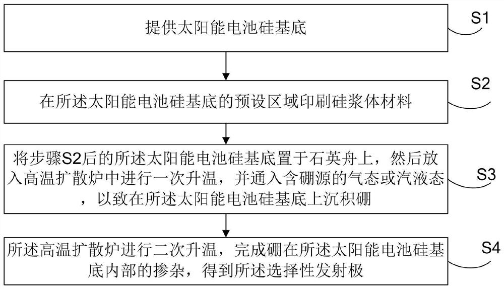
[0032] refer to figure 1 , which shows a method for preparing a selective emitter provided by an embodiment of the present invention, including:
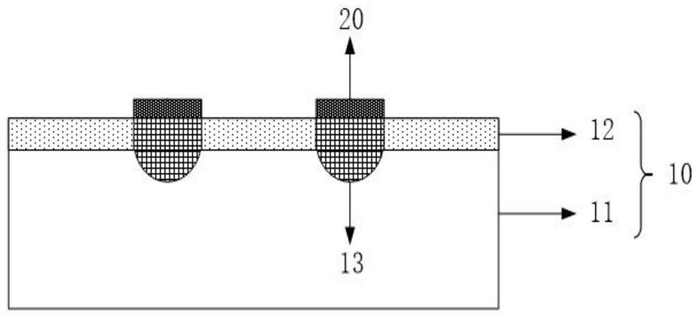
[0033] S1, providing a silicon substrate 10 for a solar cell.
[0034] In the embodiment of the present invention, refer to figure 2 , wherein the solar cell silicon substrate 10 is cleaned, and the surface morphology of the solar cell silicon substrate 10 includes: texturing, etching or polishing.
[0035] S2, printing silicon paste material 20 on a predetermined area of the silicon substrate of the solar cell.
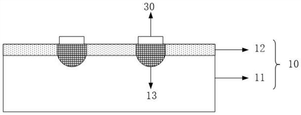
[0036] Among them, refer to figure 2 and 3 , the preset area means that after the preparation of the selective emitter is completed, the metal electrode should be prepared on the corresponding area. After the preparation of the selective emitter is completed, the redundant silicon paste material 20 is cleaned, and after cleaning, the metal electrode 30 is prepared in a predetermined area.
[0037] In the embodime...
Embodiment 2
[0052] Figure 4It shows that the embodiments of the present invention provide another aspect of the present invention to provide a method for preparing a selective emitter, the method comprising:
[0053] S1, providing a solar cell silicon substrate.
[0054] In the embodiment of the present invention, the surface topography of the silicon substrate of the solar cell includes: texturing, etching or polishing.
[0055] refer to figure 2 , wherein the solar cell silicon substrate 10 is cleaned,
[0056] S2, printing a silicon paste material containing boron particles on a predetermined area of the silicon substrate of the solar cell.
[0057] In an embodiment of the present invention, the boron-containing particles include: boron or boron oxide. Wherein, the silicon paste material containing boron particles includes: nanometer silicon powder, organic solvent and boron or boron oxide.
[0058] The particle size of the nano silicon powder is 1nm-5000nm; the organic solven...
PUM
| Property | Measurement | Unit |
|---|---|---|
| Particle size | aaaaa | aaaaa |
| Width | aaaaa | aaaaa |
Abstract
Description
Claims
Application Information
 - R&D
- Intellectual Property
- Life Sciences
- Materials
- Tech Scout
- Unparalleled Data Quality
- Higher Quality Content
- 60% Fewer Hallucinations
Browse by: Latest US Patents, China's latest patents, Technical Efficacy Thesaurus, Application Domain, Technology Topic, Popular Technical Reports.
© 2025 PatSnap. All rights reserved.Legal|Privacy policy|Modern Slavery Act Transparency Statement|Sitemap|About US| Contact US: help@patsnap.com