Supercharge Your Innovation With Domain-Expert AI Agents!

N-type GaAs ohmic contact electrode material and preparation method thereof

An ohmic contact electrode, n-type technology, applied in metal material coating process, circuits, electrical components, etc., can solve the problems of high equipment cost, troublesome cleaning, high vacuum degree, etc., to achieve low equipment cost and no waste of electrode materials. , The effect of electrode composition uniformity

Pending Publication Date: 2022-03-01
HUAIYIN TEACHERS COLLEGE
View PDF4 Cites 0 Cited by
  • Summary
  • Abstract
  • Description
  • Claims
  • Application Information

AI Technical Summary

Problems solved by technology

The disadvantage of this method is that a high degree of vacuum is required to prevent the oxidation of the alloy during evaporation, and the mechanical pump cannot meet the requirements, and a molecular pump must be equipped, resulting in high equipment cost.
Moreover, during the evaporation process, the material diffuses into the entire cavity, causing serious waste and troublesome cleaning

Method used


Image

  • N-type GaAs ohmic contact electrode material and preparation method thereof
  • N-type GaAs ohmic contact electrode material and preparation method thereof
  • N-type GaAs ohmic contact electrode material and preparation method thereof

Examples


Embodiment 1

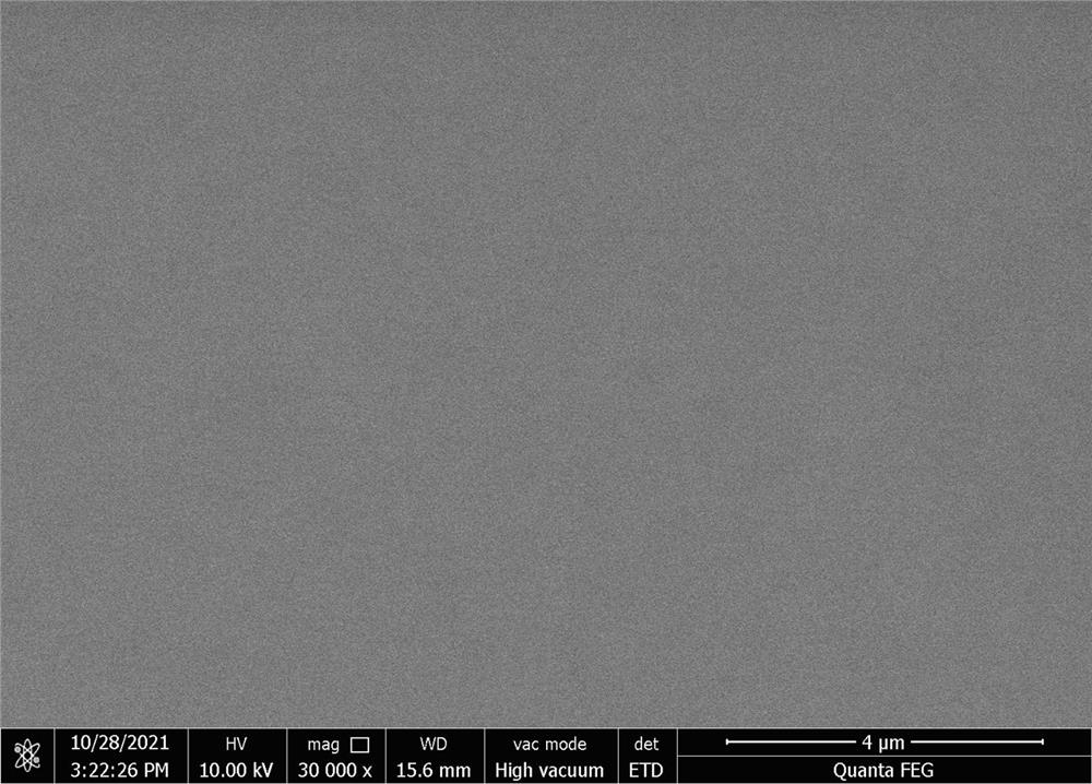
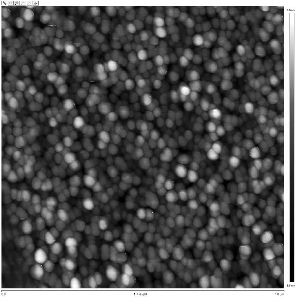
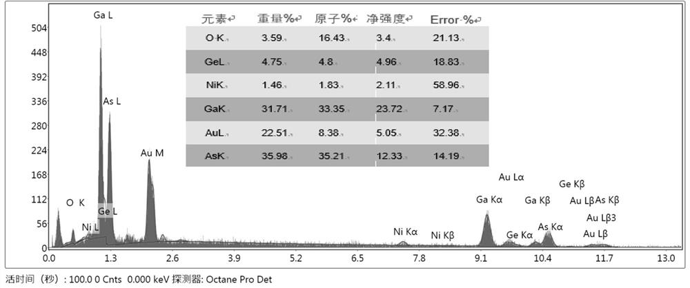
[0024] Two electrode regions were set on the n-type GaAs substrate by mask method, and AuGeNi alloy was firstly sputtered by ion sputtering method: the distance between the AuGeNi alloy target and the substrate was 5 cm. Turn on the mechanical pump, vacuum the chamber to 2Pa, pour in air and adjust the pressure in the chamber to 6 Pa to start sputtering. During the sputtering process, the current is kept at 5 mA by fine-tuning the pressure, and the thickness of the AuGeNi alloy layer needs to reach 50~70 nm . Then sputter gold Au: the distance between the gold Au target and the substrate is 7 cm, turn on the mechanical pump, evacuate the chamber to 2 Pa, pour air into the chamber to adjust the pressure in the chamber to 6 Pa, and start sputtering. The sputtering process passes Fine-tune the air pressure to keep the current at 5 mA, and the thickness of the Au layer must reach 100-120 nm. After the electrode thickness reaches the requirement, move the substrate to the tube ann...


PUM

PropertyMeasurementUnit
thicknessaaaaaaaaaa
thicknessaaaaaaaaaa
surface roughnessaaaaaaaaaa

Abstract

The invention discloses an n-type GaAs ohmic contact electrode material and a preparation method thereof.The n-type GaAs ohmic contact electrode material is characterized in that two electrode areas are arranged on an n-type GaAs substrate through a mask method, AuGeNi alloy is firstly sputtered in the two electrode areas through an ion sputtering method, then Au is sputtered in the two electrode areas, and two corresponding AuGeNi / Au electrode structures are formed; and finally, performing high-temperature annealing to obtain the n-type GaAs stable ohmic contact electrode. Through detection, the n-type GaAs ohmic contact electrode prepared by the method is uniform in electrode component and flat and smooth in surface. An I-V curve between the two electrodes has a good linear and symmetrical relation, the resistivity of the electrodes is far smaller than that of a GaAs substrate, the performance indexes of the electrodes meet the electrode requirement for stable contact, and the electrodes can be successfully applied to n-type GaAs related devices. Compared with a manufacturing process in the prior art, the method disclosed by the invention is low in equipment cost and short in process, saves electrode materials, has good economic benefits and practical value, and is particularly suitable for scientific research laboratories.

Description

technical field [0001] The invention belongs to the field of optoelectronic technology and relates to the preparation of a semiconductor material, in particular to an n-type GaAs ohmic contact electrode material and a preparation method thereof. Background technique [0002] Gallium arsenide (GaAs) is a III-V compound semiconductor with a zinc blende crystal structure. It has some properties superior to silicon and has become an important semiconductor material second only to silicon. It can be made into a semi-insulating high-resistance material whose resistivity is more than 3 orders of magnitude higher than that of silicon and germanium, and is used in photoconductive switches, integrated circuit substrates, infrared detectors, gamma photon detectors, etc. In addition, gallium arsenide has six times higher electron mobility than silicon, making it essential for ultra-high-speed, ultra-high-frequency devices and integrated circuits. It is also widely used in the military...

Claims


Application Information

Patent Timeline
Patent Type & Authority Applications(China)
IPC IPC(8): H01L31/0224H01L31/18C23C14/18
CPCH01L31/0224H01L31/022408H01L31/18C23C14/18Y02P70/50
Inventor 翟章印左芬边心田
Owner HUAIYIN TEACHERS COLLEGE
Features
  • R&D
  • Intellectual Property
  • Life Sciences
  • Materials
  • Tech Scout
  • Unparalleled Data Quality
  • Higher Quality Content
  • 60% Fewer Hallucinations
Learn More