Leadless packaging structure and method of high-temperature-resistant sensor

A technology of packaging structure and high temperature resistance, applied in the direction of microstructure technology, microstructure devices, manufacturing microstructure devices, etc., to reduce the possibility of thermal stress mismatch, eliminate response time lag, and low process difficulty

Pending Publication Date: 2022-03-04
XI AN JIAOTONG UNIV
View PDF3 Cites 2 Cited by
  • Summary
  • Abstract
  • Description
  • Claims
  • Application Information

AI Technical Summary

Problems solved by technology

[0007] In order to solve the technical problems existing in the existing packaging structure of high temperature resistant sensors, the present invention provides a leadless packaging structure and method for high temperature resistant sensors

Method used


Image

  • Leadless packaging structure and method of high-temperature-resistant sensor
  • Leadless packaging structure and method of high-temperature-resistant sensor
  • Leadless packaging structure and method of high-temperature-resistant sensor

Examples


Embodiment 1

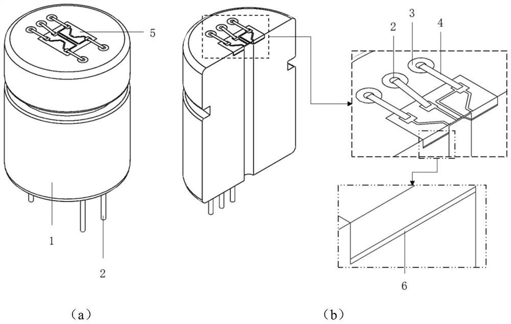
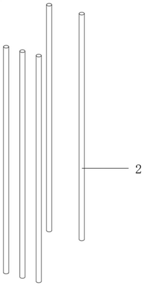
[0049] Such as figure 1 As shown, the overall packaging structure of the high temperature resistant sensor includes a sensor housing 1 , metal pins 2 and a sensor chip 5 . A part of the metal pin 2 is fixed inside the sensor housing 1 through the conductive sealing block 3 formed by the cured conductive glass paste, and the sensor chip 5 is fixed in the sealing layer formed by the cured high temperature resistant adhesive. 6 is fixed on the upper end surface of the sensor housing 1 in a fitting manner; wherein, the sensor chip 5 faces upward, and the upper end of the metal pin 2, the cured conductive glass paste, and the front surface of the sensor chip 5 are all in contact with the sensor housing. 1 is flush with the upper end surface, the lower end of the metal pin 2 protrudes out of the lower end surface of the sensor housing 1 , and the back of the sensor chip 5 is opposite to the channel or cavity structure inside the sensor housing 1 . On the junction of the upper end s...

Embodiment 2

[0088] The above embodiment 1 is aimed at the relatively friendly working environment of the sensor chip, for example, the situation that the chip is not in direct contact with water vapor, dust or corrosive substances. If the sensor chip works in an environment containing water vapor, dust or corrosive substances, it is necessary to consider using the packaging structure to protect the circuit structure on the front of the sensor chip, so Embodiment 2 is proposed.

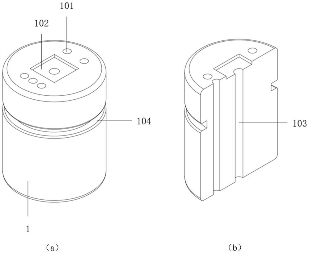
[0089] Such as Figure 5 As shown in a, the main difference between the overall packaging structure of the high temperature resistant sensor of this embodiment and that of Embodiment 1 is that the sensor chip 5 is placed upside down in the chip packaging groove 102, that is, the back of the sensor chip 5 faces upward, and the circular through hole 101 The layout positions on the end surface of the sensor housing 1 are all located inside the chip packaging groove 102, that is, the upper end of the circular through ...


PUM


Abstract

The invention discloses a leadless packaging structure and method of a high-temperature-resistant sensor, the leadless packaging structure comprises a sensor chip, a sensor shell used for supporting the sensor chip and a metal pin arranged on the sensor shell, the metal pin is connected with a metal electrode of the sensor chip through a high-temperature-resistant conductive layer, and the metal electrode is connected with the sensor chip through a high-temperature-resistant conductive layer. And the metal electrode is externally arranged on the surface of the sensor shell or is internally arranged in the sensor shell. According to the invention, on one hand, the problem of reliability degradation and even failure of a conventional metal lead bonding packaging technology in a high-temperature environment is solved, on the other hand, the lead packaging mode is simplified, the operation is simple, the yield is high, the reliability in actual use is high, the method is suitable for batch production, the cost is low, and the cost performance is very high. Meanwhile, by selecting and simplifying packaging materials, the working stability and long-term reliability of the sensor in a high-temperature environment are improved, and the sensor chip has the advantage of being good in dynamic response characteristic by adopting flush packaging.

Description

technical field [0001] The invention relates to a high temperature resistant sensor, in particular to a leadless packaging structure and method of the sensor. Background technique [0002] High temperature resistant sensors have very important applications in many industries and fields, such as high temperature resistant pressure and vibration sensors for internal high temperature pressure and vibration detection of aeroengines, high temperature resistant pressure sensors for primary circuit pressure measurement of high temperature reactors in nuclear power plants, and high temperature resistant pressure sensors for high temperature High-temperature pressure and vibration sensors for operational safety monitoring of industrial reactors and smelting towers. [0003] The key reason why the high temperature resistant sensor can work normally in high temperature environment is: (1) the sensor chip itself can work normally in high temperature environment, (2) the sensor package s...

Claims


Application Information

Patent Timeline
Patent Type & Authority Applications(China)
IPC IPC(8): B81B7/00B81B7/02B81C1/00
CPCB81B7/02B81B7/007B81C1/00301B81C1/00261
Inventor 赵友赵玉龙王鲁康杨玉
Owner XI AN JIAOTONG UNIV
Why Eureka
Try Eureka