Method for detecting electric field effect of quantum dots
A technology of electric field effect and quantum dots, which is applied in the direction of measuring electricity, measuring electrical variables, measuring devices, etc., can solve the problems of long measurement preparation time, high cost, low degree of utilization, etc., and achieves simple structure, reduced detection cost, and easy production. Effect
- Summary
- Abstract
- Description
- Claims
- Application Information
AI Technical Summary
Problems solved by technology
Method used
Image

Examples
Embodiment Construction
[0015] The present invention will be described in detail below in conjunction with the accompanying drawings.
[0016] Step (1) Making the substrate: select transparent material as the substrate material, process it into a cube with a length of 2-3 mm, a width of 1-2 mm, and a height of 0.1-1 mm, wash and dry it with acetone and deionized water to obtain the substrate; transparent The material is quartz or glass;
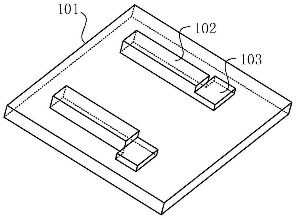
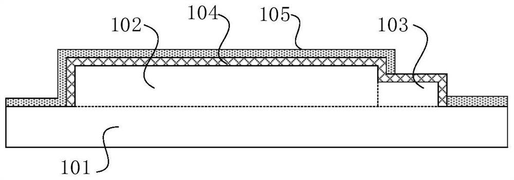
[0017] Step (2) Fabricate the electrode structure: draw the pattern of electrodes and pins on the substrate by photolithography, and then etch the required electrode structure by etching, that is, etch the substrate downward to form the electrode structure. Such as figure 1 As shown, the electrode structure includes two electrode protrusions 102 on one side of the base 101 and corresponding pin protrusions 103; the length of the strip-shaped electrode protrusions is 1-1.5mm, the width is 0.2-0.3mm, and the height 0.02 ~ 0.1mm, two electrode protrusions are arrange...
PUM
| Property | Measurement | Unit |
|---|---|---|
| Length | aaaaa | aaaaa |
| Width | aaaaa | aaaaa |
| Height | aaaaa | aaaaa |
Abstract
Description
Claims
Application Information