Shield gate groove type field effect transistor and preparation method thereof

A field effect transistor and shielded gate technology are applied in the field of shielded gate trench type field effect transistors and their preparation, and can solve the problems of increased breakdown voltage and the like

Pending Publication Date: 2022-03-04
无锡先瞳半导体科技有限公司
View PDF0 Cites 1 Cited by
  • Summary
  • Abstract
  • Description
  • Claims
  • Application Information

AI Technical Summary

Problems solved by technology

The limitation of the breakdown voltage mainly comes from the inhomogeneity of the electric field distribution in the withstand voltage region. In the traditional trench type shielded gate transistor, due to the heavy doping concentration of the shielded gate str

Method used


Image

  • Shield gate groove type field effect transistor and preparation method thereof
  • Shield gate groove type field effect transistor and preparation method thereof
  • Shield gate groove type field effect transistor and preparation method thereof

Examples


Embodiment 1

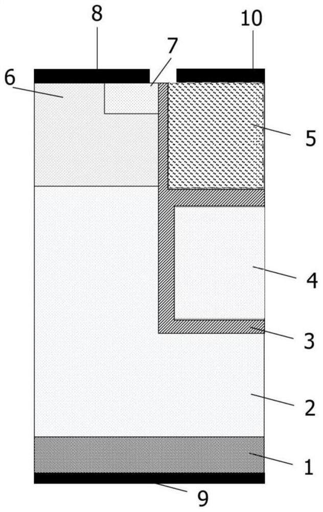
[0045] In traditional trench-type shielded gate transistors, because the doping concentration of the shielded gate structure is heavily doped, when the device is in forward blocking, the electric flux of ionized donor charges in the withstand voltage region tends to concentrate on the corner of the shielded gate. , so the larger peak electric field limits the increase in breakdown voltage.

[0046] In view of the above problems, an embodiment of the present application provides a shielded gate trench type field effect transistor, which can effectively improve the peak electric field introduced by the electric field concentration effect caused by the small curvature radius at the corner of the shielded gate.

[0047] The technical solutions of the embodiments of the present application are described in detail below with reference to the accompanying drawings.

[0048] figure 1 It is a schematic diagram of the first structure of the shielded gate trench type field effect transi...

Embodiment 2

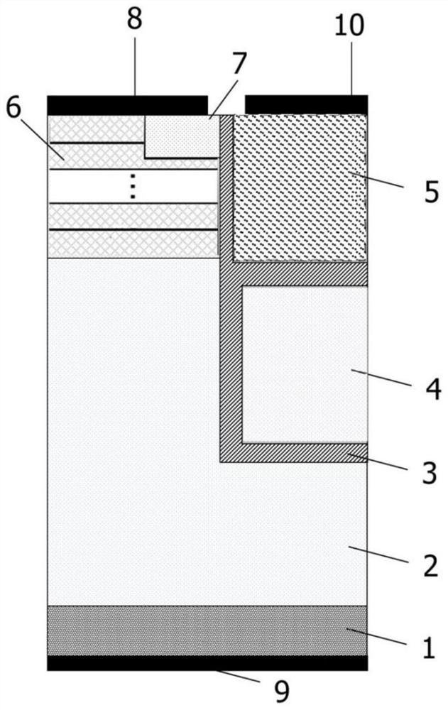
[0062] The first embodiment above provides a shielded gate trench field effect transistor. By adjusting the original heavily doped polysilicon type shielded gate structure, the peak electric field at the corner of the shielded gate is eliminated, and the polysilicon with reduced doping concentration is used It can withstand the built-in potential between the P-type polysilicon and the N-type drift region, which can reduce the lateral depletion formed between the two, thereby reducing the specific on-resistance of the device drift region, but when the breakdown voltage is less than 300V, Especially when the breakdown voltage is less than 100V, even less than 40V, the channel region and the drift region have comparable specific on-resistance. Therefore, for low-voltage shielded gate trench field effect transistors, the channel The improvement of the specific on-resistance of the channel region is as important as the design of the drift region. Therefore, the embodiment of the pr...

Embodiment 3

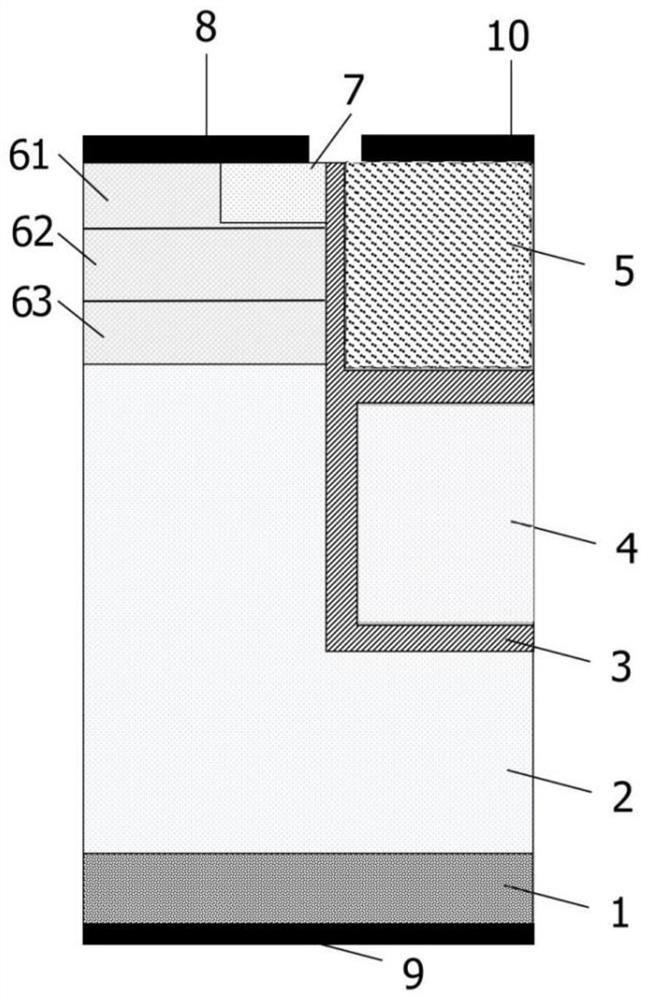
[0073] Based on the shielded gate trench field effect transistor shown in the second embodiment above, the embodiment of the present application provides a shielded gate trench field effect transistor having three doping distribution layers distributed at equal intervals.

[0074] see image 3 , the shielded gate trench field effect transistor, comprising: a substrate region 1, a drift region 2, a shielded gate 4, a control gate 5, a base region 6, a source region 7, an insulating layer 3, a source electrode 8, and a drain electrode 9 and a metal grid 10;

[0075] Wherein, the drift region 2 , the base region 6 , the source region 7 and the source 8 are sequentially disposed above the substrate region 1 , and the drain 9 is disposed below the substrate region 1 , the control gate 5 and the shielding gate 4 are arranged on the same side of the drift region 2 from top to bottom, and the control gate 5 is respectively connected to the base region 6 and the source through the ins...


PUM

PropertyMeasurementUnit
Doping concentrationaaaaaaaaaa
Thicknessaaaaaaaaaa

Abstract

The invention relates to a shield gate trench type field effect transistor and a preparation method thereof. The transistor comprises a substrate region, a drift region, a shield gate, a control gate, a matrix region, a source region, an insulating layer, a source electrode, a drain electrode and a metal gate electrode, the drift region, the base region, the source region and the source electrode are sequentially arranged above the substrate region, the drain electrode is arranged below the substrate region, and the control gate and the shield gate are arranged on one side of the drift region from top to bottom; the substrate region, the drift region and the source region are all N-type doped; the doping concentration of the substrate region and the doping concentration of the source region are both larger than the doping concentration of the drift region. The substrate region, the shield gate and the control gate are all P-type doped; the doping concentration of the shield grid is the same as that of the drift region; and the doping concentration of the control grid is greater than that of the shielding grid. According to the scheme provided by the invention, a peak electric field introduced by an electric field concentration effect caused by a relatively small curvature radius at a corner of the shielding grid can be effectively improved, and an effect of improving a breakdown voltage is achieved, so that the specific on-resistance of the device is reduced.

Description

technical field [0001] The present application relates to the field of semiconductor technology, in particular to a shielded gate trench type field effect transistor and a preparation method thereof. Background technique [0002] Compared with the traditional trench transistor, the shielded gate trench field effect transistor has higher channel density and better charge compensation effect, and its shielded gate structure effectively reduces the transfer capacitance, so it has a lower ratio On-resistance, smaller conduction and switching losses, and higher operating frequency are widely used in important fields such as power management. [0003] In related technologies, the contradictory relationship between breakdown voltage and specific on-resistance is an extremely important physical parameter in power devices, especially for unipolar power devices. The limitation of the breakdown voltage mainly comes from the inhomogeneity of the electric field distribution in the withs...

Claims


Application Information

Patent Timeline
IPC IPC(8): H01L29/78H01L21/336H01L29/423H01L29/06
CPCH01L29/7827H01L29/7831H01L29/66666H01L29/66484H01L29/4236H01L29/0611
Inventor 张子敏王宇澄虞国新吴飞钟军满
Owner 无锡先瞳半导体科技有限公司
Why Eureka
Try Eureka