1342 nanometer wavelength high-power microstructure DFB laser

A DFB laser, laser technology, applied in lasers, laser parts, semiconductor lasers, etc., can solve the problems of low yield of dual-mode lasing and single-mode, increase the difficulty and cost of the process, disadvantageous high-power output, etc. Difficulty and cost, effect of increased process difficulty, broad applicability

Active Publication Date: 2022-03-15
JIANGSU HUAXING LASER TECH CO LTD
View PDF5 Cites 0 Cited by
  • Summary
  • Abstract
  • Description
  • Claims
  • Application Information

AI Technical Summary

Problems solved by technology

[0005] The usual semiconductor DFB edge-emitting lasers have dual-mode lasing or low single-mode yield due to the use of uniform grating periodic refractive index guidance. In order to improve the single-mode output, a phase shift will be introduced, which will greatly increase the process difficulty and Cost, the conventional DFB structure is easily saturated due to the limitation of the optical mode volume, and it is not conducive to high power output

Method used


Image

  • 1342 nanometer wavelength high-power microstructure DFB laser
  • 1342 nanometer wavelength high-power microstructure DFB laser
  • 1342 nanometer wavelength high-power microstructure DFB laser

Examples


Embodiment Construction

[0047] The present invention will be specifically introduced below in conjunction with the accompanying drawings and specific embodiments.

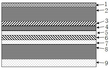
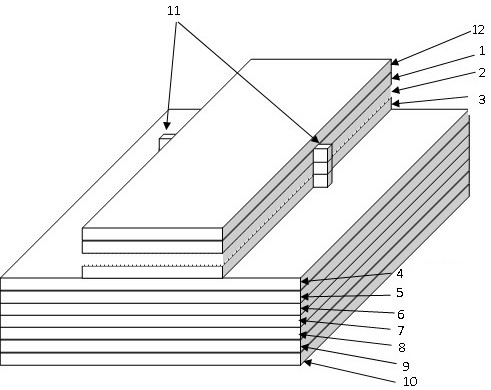
[0048] A high-power microstructure DFB laser with a wavelength of 1342 nanometers, which consists of 11 layer structures and 1 microstructure, which are the lower cover layer 8, the diluted waveguide layer 7, the lower waveguide layer 6, the multi-quantum Well active region 5, upper waveguide layer 4, grating layer 3, upper cover layer 2, contact layer 1, and insulating layer, N electrode 10 covers the bottom surface of the substrate, and P electrode 12 is arranged on the insulating layer and at the ridge strip connected to the contact layer. Such as figure 2 shown.

[0049]The lower cover layer, diluted waveguide layer, lower waveguide layer, multi-quantum well active region, and upper waveguide layer in the epitaxial material constitute stack A, and the grating layer, upper cover layer, and contact layer constitute stack B; and stack...


PUM

PropertyMeasurementUnit
thicknessaaaaaaaaaa
thicknessaaaaaaaaaa
thicknessaaaaaaaaaa

Abstract

A high-power microstructure DFB laser with the wavelength of 1342 nanometers adopts a quantum well structure meeting the requirement for the emission wavelength of 1342 nanometers, realizes single-mode work through combination of a microstructure and a common distributed feedback grating, further introduces a multi-layer dilution waveguide structure to expand optical power output, and meets the requirement for high-power output. And the yield of the device is greatly improved on the basis of not increasing the process difficulty. The problems that due to the fact that a common semiconductor DFB edge-emitting laser adopts uniform grating periodic refractive index for guiding, dual-mode lasing or the single-mode yield is low, phase shift is introduced in order to improve single-mode output, and the process difficulty and cost are greatly increased are solved. And meanwhile, the problem that a conventional DFB structure is easy to saturate due to the limitation of the light mode volume and is not beneficial to high-power output is solved, so that the laser can be applied to 50G PON silicon light, and has very high practicability and wide applicability.

Description

technical field [0001] The invention relates to a DFB laser, in particular to a 1342nm wavelength high-power microstructure DFB laser and a manufacturing method thereof, which belong to the technical field of photonic optoelectronic devices. Background technique [0002] Semiconductor diode lasers are the most practical and important class of lasers. It is small in size, long in life, and can be pumped by simply injecting current. Its operating voltage and current are compatible with integrated circuits, so it can be monolithically integrated with it. Moreover, current modulation can be directly performed at a frequency up to tens of GHz to obtain high-speed modulated laser output. Due to these advantages, semiconductor diode lasers have been widely used in laser communications, optical storage, optical gyroscopes, laser printing, ranging, and radar; it also enables high-power applications of semiconductor lasers, such as marking, welding, cutting, etc. The pump source of ...

Claims


Application Information

Patent Timeline
Patent Type & Authority Applications(China)
IPC IPC(8): H01S5/12H01S5/343
CPCH01S5/12H01S5/34313H01S5/34306
Inventor 徐鹏飞王文知王岩罗帅季海铭
Owner JIANGSU HUAXING LASER TECH CO LTD
Why Eureka
Try Eureka